PR Newswire: OmniVision announces a cost-efficient and compact 720p30 HD CameraChip sensor, designed for secondary cameras in notebooks, tablets and smartphones, as well as the rapidly developing smart TV market. The new OV9728 utilizes a 1.75um OmniBSI+ pixel that exceeds the Microsoft Lync and Skype specifications for video quality.
"The exploding demand for HD cameras across a wide range of applications has been the key driver for developing this high performance, low-cost and low-power HD camera solution," said Archie de Guzman , senior product marketing manager at OmniVision. "Two years ago, when we launched the previous-generation OV9726 sensor, Internet and broadcast TV were just transitioning to HD video. Today, with HD video now prevalent, we are bringing to market a device with exceptional HD video performance at a highly competitive price point, which we view as extremely attractive for a very broad base of mobile and portable devices."
When compared with the previous-generation OV9726, the new OV9728 benefits from a 60% improvement in FWC, a 4db improvement in DR, and a significantly enhanced SNR that meets Microsoft's recommended SNR10 standards. The 1/6.5-inch OV9728 has one-lane high-speed MIPI interface and fits into a compact 6 x 6 x 3 mm module. It is currently available for sampling and is expected to enter volume production in the third quarter of 2013.
PR Newswire: Another new HD video sensor targets mobile front-facing camera applications and is based on 1.34um OmniBSI-2 pixel. The new 1/6-inch OV2724 delivers 1080p60 video and fits inside a 5 x 5 x 3.5 mm module. The OV2724 features a dual-lane MIPI interface and is available in chip scale package (CSP) and reconstructed wafer (RW) formats. The sensor is currently sampling and is expected to enter mass production in the third quarter of calendar 2013.
Tuesday, April 30, 2013
Pelican Raises $20M from Qualcomm, Nokia Growth Partners, and Current Investors
PR Newswire: It's official now, Pelican Imaging announces the closing of $20M in Series C funding. New strategic investors include Qualcomm Inc., acting through its venture investment group, Qualcomm Ventures, and Nokia Growth Partners, and the round includes existing venture investors Globespan Capital Partners, Granite Ventures, InterWest Partners and IQT.
"We're excited to take the company to the next level," said Pelican Imaging CEO and President Christopher Pickett . "The support from industry leaders like Qualcomm Ventures and NGP really underscores the validity of our technology in the marketplace. The continued backing from our current investors is a reflection of their confidence in our technology and our ability to execute in order to disrupt the mobile photography space."
Pelican's computational camera technology provides depth mapping at every pixel, allowing users to perform a range of selective focus and edits, both pre- and post-capture. The camera itself is said to be about 50% thinner than existing mobile cameras.
Nokia Growth Partners Managing Partner Bo Ilsoe says: "Pelican Imaging's computational camera solutions are at the cutting edge of mobile camera technologies. We believe they're positioned to lead the next wave in video and image capture; they're a great addition to our portfolio of innovators in the imaging space."
Nokia Growth Partners to Invest in Pelican Imaging
Bloomberg: Nokia Growth Partners plans to invest in Pelican Imaging seeking to win back customers from Apple and Android phones. Image quality is one of the top three reasons to buy or return a phone, and as Nokia phones are known for their cameras, it’s seen as a good leverage point, according to Nokia Growth Partners.
Array cameras "are on the cusp of being commercialized and Pelican does software for that," Bo Ilsoe, a partner at Nokia Growth Partners, said in a phone interview from California. "It’s very complicated to do this algorithmically and Pelican is one of the companies that has mastered this technology." Nokia Growth Partners has been tracking Pelican since soon after its founding in 2008, Ilsoe said. Pelican also counts Globespan Capital Partners, Granite Ventures, InterWest Partners and IQT among its private-equity investors.
Array cameras "are on the cusp of being commercialized and Pelican does software for that," Bo Ilsoe, a partner at Nokia Growth Partners, said in a phone interview from California. "It’s very complicated to do this algorithmically and Pelican is one of the companies that has mastered this technology." Nokia Growth Partners has been tracking Pelican since soon after its founding in 2008, Ilsoe said. Pelican also counts Globespan Capital Partners, Granite Ventures, InterWest Partners and IQT among its private-equity investors.
Monday, April 29, 2013
David Orton to Deal with Image Processing
Business Wire: GEO Semiconductor announces that David Orton, formerly CEO of Aptina, has joined the GEO board of directors. In addition to serving on GEO’s board, Mr. Orton will chair a newly formed Strategic Committee to help shape GEO’s business strategy and evaluate additional ways to leverage its intellectual property assets.
GEO deals with programmable, high performance geometric processor ICs featuring the highly acclaimed and patented eWarp geometric processor, H.264 CODECS, as well as video, audio and human interface technologies for automotive, mobile, and security markets. GEO used to cooperate with Aptina.
GEO’s Chairman and CEO, Paul Russo, says "We are... pleased to welcome Dave to our board. Dave is a semiconductor veteran that truly understands the high growth automotive and cloud camera markets, which are key target markets for GEO. His vast experience from serving as CEO of Aptina, a world-class CMOS image sensor manufacturer, and ATI will be invaluable as we further mold GEO’s strategy."
"GEO is well-positioned in high-growth market segments and have the breadth of IP to deliver compelling solutions as well as win business at the top-tier customers. I look forward to working with Paul and the rest of this exceptional management team," said David Orton.
Teledyne DALSA Cameras to Adopt CMOSIS Sensors
It was brought to my attention that Teledyne DALSA new Genie TS cameras are based on the CMOSIS imaging sensors CMV2000 (2M) and CMV4000 (4MP). The monochrome cameras are aimed to machine vision applications, operate at up to 76fps speed in HD format and feature HDR mode.
Fraunhofer Demoed HDR Video Method at NAB
Fraunhofer Digital Cinema NAB 2013 presentation included "HDR Video with Single Shot Non-Regular Sampling". Fraunhofer IIS scientists placed a special non-regular neutral density filter mask with different attenuations in front of the camera sensor. This makes it possible to capture dark and bright image parts at the same time, where some HDR methods need to take two or more images. The non-regular alignment of the attenuations is said to allow a near lossless reconstruction of the missing pixels in the corresponding dark or bright image. After the reconstruction, the images can be fused together to an HDR image with no motion artifacts:
Sony Sensors inside Galaxy S4, Xperia Tablet Z
Chipworks' teardown revealed Sony sensors in primary cameras of both Sony Xperia Tablet Z and Samsung Galaxy S4. Note, that Samsung Galaxy S3 was known to dual source Sony and Samsung sensors.
Xperia secondary camera is made by Sony too and uses 1.12um pixel, the first time for secondary camera in Chipworks database.
Xperia secondary camera is made by Sony too and uses 1.12um pixel, the first time for secondary camera in Chipworks database.
 |
| Camera Module based on Sony IMX111 8.2MP Sensor |
Sunday, April 28, 2013
Canon Reports Increase in Sales of Lithography Equipment for Image Sensors
Canon announces Q1'13 results and reports that "investment in semiconductor lithography equipment to produce image sensors... showed steady growth."
IMS Research Predicts Big Market for Smart Glass Devices
IHS IMS Research forecasts the global market for smart glasses, like Google Glass, could amount to almost 10 million units from 2012 through 2016. Shipments of smart glasses may rise to as high 6.6 million units in 2016, up from just 50,000 in 2012, for a total of 9.4 million units for the five-year period, according to an upside forecast from IMS Research, now part of IHS. Growth this year will climb 150 percent to 124,000 shipments, mostly driven by sales to developers. Expansion will really begin to accelerate in 2014 with the initial public availability of Google Glass, as shipment growth powers up to 250 percent, based on the optimistic forecast.
However, it all depends on applications development for such glasses. Under a more pessimistic scenario, IHS forecasts that only about 1 million smart glasses will be shipped through 2016. According to this outlook, applications for smart glasses will be limited to some of those already displayed by Google in its Glass marketing.

However, it all depends on applications development for such glasses. Under a more pessimistic scenario, IHS forecasts that only about 1 million smart glasses will be shipped through 2016. According to this outlook, applications for smart glasses will be limited to some of those already displayed by Google in its Glass marketing.
Saturday, April 27, 2013
Omnivision Proposes Combined Buried-Surface TG Structure
Omnivision patent application US20130092982 "Partial buried channel transfer device for image sensors" by Gang Chen, Sing-Chung Hu, Hsin-Chih Tai, Duli Mao, Manoj Bikumandla, Wei Zheng, Yin Qian, Zhibin Xiong, Vincent Venezia, Keh-Chiang Ku, and Howard Rhodes proposes to have additional doping on TG making its adjacent to PD part to be buried-channel:


"The result is that any dark current generated under transfer device 425 is likely to drift toward floating diffusion region 415. This feature prevents white pixels from forming and reduces image lag by discouraging electrons from being sent back to photosensitive element 410 after a transfer event."


"The result is that any dark current generated under transfer device 425 is likely to drift toward floating diffusion region 415. This feature prevents white pixels from forming and reduces image lag by discouraging electrons from being sent back to photosensitive element 410 after a transfer event."
Boston Bombing to Boost Security Camera Sales
EETimes quotes IHS' IMS Research predicting Boston bombing to spur a dramatic increase in video surveillance camera sales. "While it’s too early to tell exactly what impact the Boston bombing will have, past events—like 9/11 and the London Underground bombings—have led to increased government spending on video surveillance for public spaces, particularly in the transport sector," said Paul Everett, senior manager of video surveillance at IHS.
The older, pre-bombing IMS Research's PR on Video Surveillance Trends for 2013 can be found here.
The older, pre-bombing IMS Research's PR on Video Surveillance Trends for 2013 can be found here.
Friday, April 26, 2013
How to Measure Non-Linearity
Albert Theuwissen continues his excellent "How to Measure..." series of articles. The latest 3 articles talk about the non-linearity measurements. Starting from a general discussion of non-linearity effects, the series continues with INL measurements and testing it at different gain settings. The non-linearity is such a rich phenomenon that one can devote a lot of articles to it, such as image lag influencing non-linearity, difference in 3T and 4T pixel nonlinearity effects, dynamic and static pictures nonlinearity, nonlinearity in different types of global shutter pixels as compared with the regular rolling shutter ones, strong light/short exposure vs low light/long exposure non-linearity, and, probably, more. So, I think it has all the chances to be a very educating series, stay tuned.
Pyxalis Update
There has been little public information about Pyxalis since it has been founded in 2010. Now Yole's Micronews #143 publishes a sort of update on the company progress and plans:
Pyxalis’ design portfolio includes work and intellectual property in the HDR capture; global shutter or rolling shutter pixels; high-speed imaging; low-light imaging and near-infrared (NIR) sensitivity; embedded image processing; very large area image arrays with only one chip per wafer for use in medical and nondestructive testing applications; and high-performance column ADC architectures with up to 14-bit resolution. "In terms of technology development, we’re focusing on innovative and distinct features at the image sensor levels and, for example, provide a range of high-performance fast ADCs with high resolution—ranging from 8 to 14 bits now, and we’ll expand that range in the future,” says Pyxalis CEO Philippe Rommeveaux.
For image processing, Pyxalis integrates an on-chip 32-bit microcontroller. "By using the microcontroller to do preprocessing on-chip, it means that signal conditioning and calculations—as well as image quality improvements—can be done directly on chip," explains Rommeveaux.
Pyxalis’ goal for the next few years is to continue its growth trajectory and to be a long-term design house. "We currently have 15 employees, and our target is to grow by 2x during the next three to four years," says Rommeveaux. "And we intend to continue innovating in the CMOS image sensor design field, with a strong commitment to quality service and time-to-product."
CEVA Pushes Super-Resolution to Mainstream
PR Newswire: CEVA, the licensor of DSP cores IP, introduces what it says the world's first software-based Super-Resolution (SR) Technology for embedded applications, bringing PC system-equivalent imaging performance to low power mobile devices. The Super-Resolution algorithm is optimized to run in real-time using minimal processing workload and very low memory bandwidth on the CEVA-MM3101 imaging and vision platform. For example, in a 28nm process, the CEVA-MM3101 processor is able to take four 5MP images and fuse them into a single high-resolution 20MP image in a fraction of a second, while consuming less than 30mW.
CEVA's Super-Resolution algorithm enables the creation of high resolution images using low resolution image sensors and allows high-quality digital zoom in real-time on mobile devices. Traditionally, such applications were only available on PC systems, limited to offline processing of pre-captured images.
Eran Briman , VP marketing at CEVA says: "Our new Super-Resolution algorithm for the CEVA-MM3101 platform marks the first time that this technology is available in software for embedded applications. It is a testament to both the expertise of our highly skilled software engineers and to the low power capabilities of our CEVA-MM3101 platform, which comprises the hardware platform together with optimized algorithms, software components, kernel libraries, software multimedia framework and a complete development environment. We continue to lead the industry in the embedded imaging and vision domain and the addition of this latest high performance software component to our platform furthers illustrates the strength of our IP portfolio for advanced multimedia applications."


Update: Once we are at HDR and Super-Resolution algorithms, Chalmers University of Technology, Sweden published a fresh thesis "Towards Joint Super-Resolution and High Dynamic Range Image Reconstruction" by Tomas Bengtsson.
CEVA's Super-Resolution algorithm enables the creation of high resolution images using low resolution image sensors and allows high-quality digital zoom in real-time on mobile devices. Traditionally, such applications were only available on PC systems, limited to offline processing of pre-captured images.
Eran Briman , VP marketing at CEVA says: "Our new Super-Resolution algorithm for the CEVA-MM3101 platform marks the first time that this technology is available in software for embedded applications. It is a testament to both the expertise of our highly skilled software engineers and to the low power capabilities of our CEVA-MM3101 platform, which comprises the hardware platform together with optimized algorithms, software components, kernel libraries, software multimedia framework and a complete development environment. We continue to lead the industry in the embedded imaging and vision domain and the addition of this latest high performance software component to our platform furthers illustrates the strength of our IP portfolio for advanced multimedia applications."
 |
| Click to expand |
 |
| Click to expand |
 |
| Click to expand. Somehow does not show a significant improvement in resolution. May be the 4 component images were shot from tripod by mistake? |


Update: Once we are at HDR and Super-Resolution algorithms, Chalmers University of Technology, Sweden published a fresh thesis "Towards Joint Super-Resolution and High Dynamic Range Image Reconstruction" by Tomas Bengtsson.
Thursday, April 25, 2013
SiOnyx to Demo XQE Sensors
Business Wire: SiOnyx announces the first public demonstration of its XQE family of image sensors at SPIE Defense, Security, and Sensing. XQE image sensors are said to "deliver unprecedented performance advantages in infrared imaging with sensitivity enhancements as high as 10x incumbent solutions. In addition, SiOnyx XQE sensors deliver true nightglow detection capabilities in extreme, low-light conditions." SiOnyx VP Engineering and CTO, Homayoon Haddad, will present the capabilities of the XQE sensors and discuss their technical specifications.
"SiOnyx, in collaboration with our foundry partners, has created an entirely new category of CMOS image sensor," said Haddad. "Extraordinary sensitivity enhancements combined with low cost, low noise silicon manufacturing delivers stunning results."
IR sensitivity is critical in some mass-market applications, including biometrics, eye tracking, gesture recognition, and surveillance. SiOnyx XQE sensors take advantage of the naturally occurring IR 'nightglow' to enable imaging under conditions that normally require expensive image-intensified nightvision equipment. In addition, XQE sensors deliver 1064nm laser detection for laser See Spot designation and targeting applications of smart munitions in a single focal plane solution.
The XQE sensor family all share the benefits of ultra-low read noise for extended low light imaging and 72dB of native DR. Additionally, all XQE sensors have on-chip HDR features that allow up to 120dB DR capability. XQE sensors are fabricated with a standard CMOS process that offers low power, low dark current, and no sensor cooling requirements.
SiOnyx XQE image sensors are sampling in Q2 2013 to customers interested in evaluating the use of XQE image sensors in next generation imaging platforms.
Below is a video from 1.3MP XQE-1310 sensor on moonless night, 1/30s, f1.4:
Toshiba Announces 1/3-inch HDR Video Sensor
Business Wire: One more time Toshiba announces a full HD (1080p60) 1/3-inch image sensor for the security/surveillance and automotive markets featuring 2.7um pixel, HDR and color noise reduction (CNR). According to the company, the new TCM5117PL has an industry-leading DR of 100dB. The output data format is 10b in normal mode or 12b in HDR mode.
Toshiba's single-frame, alternate-row, dual-exposure HDR implementation in the TCM5117PL is said to be well suited for capturing fast-moving objects compared to conventional multi-frame systems. With frame rates at 30 fps for conventional multi-frame systems, the single-frame approach, at 60 fps, promotes faster, less blurry and higher-quality images especially in high-contrast light conditions.
Toshiba's single-frame, alternate-row, dual-exposure HDR implementation in the TCM5117PL is said to be well suited for capturing fast-moving objects compared to conventional multi-frame systems. With frame rates at 30 fps for conventional multi-frame systems, the single-frame approach, at 60 fps, promotes faster, less blurry and higher-quality images especially in high-contrast light conditions.
Wednesday, April 24, 2013
MIT Image Processing Ideas
The Institute publishes an article on MIT low power ISP presented at the recent ISSCC. There are five unique features of the new ISP:

- Very low power consumption
- Hardware implemented bilateral filtering. Consumes 17.8mW per megapixel at 0.9 V supply (not clear what's the frame rate)
- Fast HDR imaging based on 3 frame combination, processes 10MP image in few hundred ms. Said to be fast enough for video. (Sony too supports HDR video for quite a some time)
- Low light picture improvement by a combination of flash and ambient illuminated images (in development now)
- Optical glare reduction

Hyperspectral Video Camera
Imec published Vimeo video with first demonstration of its hyperspectral camera operating at video-rates. The image is captured in 32 different spectral bands in parallel at 60 data-cubes / second and analyzed in real-time with PCA (principle component analysis) discrimination algorithms:
Thanks to JB for the link!
Thanks to JB for the link!
Tuesday, April 23, 2013
Samsung Licenses Tessera's Face Recognition Software
Business Wire: DigitalOptics Corporation (DOC), a subsidiary of Tessera, announces that Samsung has signed a multi-year license for DOC’s Face Detection and Face Tracking software. This software will be used in Samsung Galaxy S4 smartphones.
Thanks to SF for the link!
Thanks to SF for the link!
Saturday, April 20, 2013
NHK and Tokyo University Propose Dual Sided Contact in SOI FET
NHK and Tokyo University presented a nice alternative to TSV in stacked sensors on PRiME 2012 (Pasific Rim Meeting on Electrochemical and Solid-State Science) held in Honolulu, Hawaii on October 7-12, 2012:
"Development of novel MOSFET with front and back side electrodes for 3D-structured image sensors"
Masahide Goto, Kei Hagiwara, Yoshinori Iguchi, Hiroshi Ohtake, TakuyaSaraya, Hiroshi Toshiyoshi, and Toshiro Hiramoto
NHK Science and Technology Research Laboratories
The University of Tokyo
The proposal is quite simple (in a hindsight). In a multilayer image sensor structure one normally uses TSVs to transfer signals between the layers:

However, TSV size is quite big for the modern pixels of 1um size. Instead, the researchers propose a fully depleted SOI FET with front and back side contacts:

Friday, April 19, 2013
Image Sensors at VLSI Symposia 2013
VLSI Circuit Symposium to be held on June 11-14, 2013 in Kyoto, Japan has Session 2 entirely devoted to image sensors:
A 1-inch Optical Format, 14.2M-Pixel, 80fps CMOS Image Sensor with a Pipelined Pixel Reset and Readout Operation
H. Honda*, S. Osawa*, M. Shoda*, E. Pages*, T. Sato*, N. Karasawa*, B. Leichner**, J. Schoper**, E.S. Gattuso**, D. Pates**, J. Brooks**, S. Johnson**and I. Takayanagi*, *Aptina Japan and **Aptina Imaging, Japan
A 1-inch optical format, 14.2M-pixel, 80fps, digital-output CMOS image sensor that employs a row-shared dual conversion gain pixel is presented. To achieve the 80fps readout rate, a pipelined pixel reset/readout scheme named "nesting scan" has been introduced, where the charge sense node inside a pixel is reset during the previous row. Readout noise and maximum handling signal charge of the sensor are 1.7e-rms and 16ke-, respectively, and the ratio of column FPN to readout noise is lower than 0.03 in all gain conditions.
A 5.9μm-Pixel 2D/3D Image Sensor with Background Suppression over 100klx
J. Cho*, J. Choi*, S.-J. Kim**, J. Shin***, S. Park*, J.D.K. Kim*** and E. Yoon*, *University of Michigan, USA, **Institute of Microelectronics, Singapore and ***Samsung Advanced Institute of Technology, Korea
A 2D/3D image sensor with reconfigurable pixel array and column-level background suppression scheme is presented for high resolution outdoor imaging. The proposed pixel array employs pixel binning and superresolution techniques for adaptable resolution. The sensor achieved a 5.9μm pixel and was able to capture full resolution outdoor depth images under daylight over 100klx.
An Ultra-Low Noise Photoconductive Film Image Sensor with a High-Speed Column Feedback Amplifier Noise Canceller
M. Ishii, S. Kasuga, K. Yazawa, Y. Sakata, T. Okino, Y. Sato, J. Hirase, Y. Hirose, T. Tamaki, Y. Matsunaga and Y. Kato, Panasonic Corporation, Japan
We developed an ultra-low noise image sensor in which an organic photoconductive film (OPF) is laminated on the entire surface of the pixel circuits. In order to suppress the kTC noise in the pixel circuit of a three transistor configuration, a high- speed column feedback noise cancel circuit is newly developed. An ultra-low noise of 2.9 electrons during the horizontal blanking period of only 5 μs has been achieved.
A 100-fps Fluorescence Lifetime Imager in Standard 0.13-μm CMOS
R.M. Field and K.L. Shepard, Columbia University, USA
A wide-field fluorescence lifetime imager capable of up to 100 frames per second (fps) is presented. The imager consists of a 64-by-64 array of low-noise single photon avalanche diodes (SPADs) in a standard 0.13-micron CMOS process, 4096 time-to- digital converters, and an application specific data path to enable continuous image acquisition at a total output data rate of 42 Gbps. These features combine to enable new lifetime-based diagnostic imaging.
820-GHz Imaging Array Using Diode-Connected NMOS Transistors in 130-nm CMOS
D.Y. Kim*, S. Park*, R. Han** and K.K. O*, *University of Texas and **Cornell University, USA
An 820-GHz 8X8 imaging array using diode-connected NMOS transistor detectors is demonstrated in 130-nm CMOS process. Measured mean responsivity of 3.4 kilo volt per watt and mean NEP of 28 pico watt per root Hz at 1MHz modulation frequency are achieved. The NEP is 3.5X lower than that of NMOS and slightly lower than that of Schottky diode terahertz imaging arrays implemented in CMOS. The minimum NEP is 15.5 pico watt per root Hz, which is the lowest for THz detector arrays fabricated in CMOS. The imaging array occupies 2.0X1.7mm2 and the power consumption is 9.6 mW.
Session 14 too has papers on image sensors:
A 100,000 fps Vision Sensor with Embedded 535GOPS/W 256x256 SIMD Processor Array
S.J. Carey, A. Lopich, D.R.W. Barr, B. Wang and P. Dudek, The University of Manchester, United Kingdom
A vision chip operating with 1.9pJ/op efficiency has been fabricated in 0.18μm CMOS. Each of the 256x256 pixel-processors (dimensions 32x32μm) contains 14 binary and 7 analog registers coupled to a photodiode, an arithmetic logic unit, diffusion and asynchronous propagation networks. At the chip's periphery, facilities exist to allow pixel address extraction, analog or digital readout. The chip has been exploited to conduct real-time image processing operations at 100,000fps, locating a closed-shape object from amongst clutter.
A 240x180 10mW 12us Latency Sparse-Output Vision Sensor for Mobile Applications
R. Berner, C. Brandli, M. Yang, S.-C. Liu and T. Delbruck, University of Zurich and ETH Zurich, Switzerland
This paper proposes a 0.18μm CMOS vision sensor that combines event-driven asynchronous readout of temporal contrast with synchronous frame-based active pixel sensor (APS) readout of intensity. The sensor is suitable for mobile applications because it allows low latency at low data rate and therefore, low system-level power consumption. The image frames can be used for scene analysis and the temporal contrast events can be used to track fast moving objects, to adjust the frame rate or to guide a region of interest readout. Sharing the photodiode for both readout types allows a compact pixel design that is 60% smaller than a comparable technology. The 240x180 sensor has a power consumption of 10mW; the temporal contrast pathway has a minimum latency of 12us, a dynamic range of 120dB with 12% contrast detection threshold and 3.5% contrast matching; the APS readout has 57dB dynamic range with 1% FPN.
Technology Session 2 too has a nice paper on organic film sensor by Panasonic and Fujifilm:
Thin Organic Photoconductive Film Image Sensors with Extremely High Saturation of 8500 Electrons/μm2
M. Mori*, Y. Hirose*, M. Segawa*, I. Miyanaga*, R. Miyagawa*, T. Ueda*, H. Nara*, H. Masuda*, S. Kishimura*, T. Sasaki*, Y. Kato*, Y. Imada**, H. Asano**, H. Inomata**, H. Koguchi**, M. Ihama** and Y. Mishima**, *Panasonic Corporation and **FUJIFILM Corporation, Japan
We have developed an image sensor with thin organic photoconductive film (OPF) laminated on CMOS circuits. Owing to high capacity of a charge storage node, the saturation level is 12 dB higher than those of conventional image sensors. Because of the very thinness of the laminated film, i.e. 0.5 μm, the device is crosstalk-free and an incident light angle of over 30 degrees is realized.
The VLSI Symposium tip sheet gives a cross section of the 3um and 0.9um organic pixels in the paper:

The Technology Symposium has Samsung ToF paper in Session 10:
Time of Flight Image Sensor with 7μm Pixel and 640x480 Resolution
S. Kim, S. Cha, H. Park, J. Gong, Y. Noh, W. Kim, S. Lee, D.-K. Min, W. Kim, T.-C. Kim and E. Jung, Samsung Electronics Co., Ltd., Korea
Time of flight (ToF) sensor with pixel size of 7x7μm and VGA resolution is developed using a backside illumination (BSI) structure. Quantum efficiency (QE) of near infrared (NIR) light is improved dramatically by applying thick epitaxial layer, reflection metal and anti-reflection layer. The depth error ranges are 2cm and 10cm at 90% and 10% reflection condition at the distance of 7m, respectively.
Also, there is an hour-long Advanced CMOS Image Sensors lecture by Y. Egawa, Toshiba in VLSI Technology Short Course a day before the Symposia start.
A 1-inch Optical Format, 14.2M-Pixel, 80fps CMOS Image Sensor with a Pipelined Pixel Reset and Readout Operation
H. Honda*, S. Osawa*, M. Shoda*, E. Pages*, T. Sato*, N. Karasawa*, B. Leichner**, J. Schoper**, E.S. Gattuso**, D. Pates**, J. Brooks**, S. Johnson**and I. Takayanagi*, *Aptina Japan and **Aptina Imaging, Japan
A 1-inch optical format, 14.2M-pixel, 80fps, digital-output CMOS image sensor that employs a row-shared dual conversion gain pixel is presented. To achieve the 80fps readout rate, a pipelined pixel reset/readout scheme named "nesting scan" has been introduced, where the charge sense node inside a pixel is reset during the previous row. Readout noise and maximum handling signal charge of the sensor are 1.7e-rms and 16ke-, respectively, and the ratio of column FPN to readout noise is lower than 0.03 in all gain conditions.
A 5.9μm-Pixel 2D/3D Image Sensor with Background Suppression over 100klx
J. Cho*, J. Choi*, S.-J. Kim**, J. Shin***, S. Park*, J.D.K. Kim*** and E. Yoon*, *University of Michigan, USA, **Institute of Microelectronics, Singapore and ***Samsung Advanced Institute of Technology, Korea
A 2D/3D image sensor with reconfigurable pixel array and column-level background suppression scheme is presented for high resolution outdoor imaging. The proposed pixel array employs pixel binning and superresolution techniques for adaptable resolution. The sensor achieved a 5.9μm pixel and was able to capture full resolution outdoor depth images under daylight over 100klx.
An Ultra-Low Noise Photoconductive Film Image Sensor with a High-Speed Column Feedback Amplifier Noise Canceller
M. Ishii, S. Kasuga, K. Yazawa, Y. Sakata, T. Okino, Y. Sato, J. Hirase, Y. Hirose, T. Tamaki, Y. Matsunaga and Y. Kato, Panasonic Corporation, Japan
We developed an ultra-low noise image sensor in which an organic photoconductive film (OPF) is laminated on the entire surface of the pixel circuits. In order to suppress the kTC noise in the pixel circuit of a three transistor configuration, a high- speed column feedback noise cancel circuit is newly developed. An ultra-low noise of 2.9 electrons during the horizontal blanking period of only 5 μs has been achieved.
A 100-fps Fluorescence Lifetime Imager in Standard 0.13-μm CMOS
R.M. Field and K.L. Shepard, Columbia University, USA
A wide-field fluorescence lifetime imager capable of up to 100 frames per second (fps) is presented. The imager consists of a 64-by-64 array of low-noise single photon avalanche diodes (SPADs) in a standard 0.13-micron CMOS process, 4096 time-to- digital converters, and an application specific data path to enable continuous image acquisition at a total output data rate of 42 Gbps. These features combine to enable new lifetime-based diagnostic imaging.
820-GHz Imaging Array Using Diode-Connected NMOS Transistors in 130-nm CMOS
D.Y. Kim*, S. Park*, R. Han** and K.K. O*, *University of Texas and **Cornell University, USA
An 820-GHz 8X8 imaging array using diode-connected NMOS transistor detectors is demonstrated in 130-nm CMOS process. Measured mean responsivity of 3.4 kilo volt per watt and mean NEP of 28 pico watt per root Hz at 1MHz modulation frequency are achieved. The NEP is 3.5X lower than that of NMOS and slightly lower than that of Schottky diode terahertz imaging arrays implemented in CMOS. The minimum NEP is 15.5 pico watt per root Hz, which is the lowest for THz detector arrays fabricated in CMOS. The imaging array occupies 2.0X1.7mm2 and the power consumption is 9.6 mW.
Session 14 too has papers on image sensors:
A 100,000 fps Vision Sensor with Embedded 535GOPS/W 256x256 SIMD Processor Array
S.J. Carey, A. Lopich, D.R.W. Barr, B. Wang and P. Dudek, The University of Manchester, United Kingdom
A vision chip operating with 1.9pJ/op efficiency has been fabricated in 0.18μm CMOS. Each of the 256x256 pixel-processors (dimensions 32x32μm) contains 14 binary and 7 analog registers coupled to a photodiode, an arithmetic logic unit, diffusion and asynchronous propagation networks. At the chip's periphery, facilities exist to allow pixel address extraction, analog or digital readout. The chip has been exploited to conduct real-time image processing operations at 100,000fps, locating a closed-shape object from amongst clutter.
A 240x180 10mW 12us Latency Sparse-Output Vision Sensor for Mobile Applications
R. Berner, C. Brandli, M. Yang, S.-C. Liu and T. Delbruck, University of Zurich and ETH Zurich, Switzerland
This paper proposes a 0.18μm CMOS vision sensor that combines event-driven asynchronous readout of temporal contrast with synchronous frame-based active pixel sensor (APS) readout of intensity. The sensor is suitable for mobile applications because it allows low latency at low data rate and therefore, low system-level power consumption. The image frames can be used for scene analysis and the temporal contrast events can be used to track fast moving objects, to adjust the frame rate or to guide a region of interest readout. Sharing the photodiode for both readout types allows a compact pixel design that is 60% smaller than a comparable technology. The 240x180 sensor has a power consumption of 10mW; the temporal contrast pathway has a minimum latency of 12us, a dynamic range of 120dB with 12% contrast detection threshold and 3.5% contrast matching; the APS readout has 57dB dynamic range with 1% FPN.
Technology Session 2 too has a nice paper on organic film sensor by Panasonic and Fujifilm:
Thin Organic Photoconductive Film Image Sensors with Extremely High Saturation of 8500 Electrons/μm2
M. Mori*, Y. Hirose*, M. Segawa*, I. Miyanaga*, R. Miyagawa*, T. Ueda*, H. Nara*, H. Masuda*, S. Kishimura*, T. Sasaki*, Y. Kato*, Y. Imada**, H. Asano**, H. Inomata**, H. Koguchi**, M. Ihama** and Y. Mishima**, *Panasonic Corporation and **FUJIFILM Corporation, Japan
We have developed an image sensor with thin organic photoconductive film (OPF) laminated on CMOS circuits. Owing to high capacity of a charge storage node, the saturation level is 12 dB higher than those of conventional image sensors. Because of the very thinness of the laminated film, i.e. 0.5 μm, the device is crosstalk-free and an incident light angle of over 30 degrees is realized.
The VLSI Symposium tip sheet gives a cross section of the 3um and 0.9um organic pixels in the paper:
The Technology Symposium has Samsung ToF paper in Session 10:
Time of Flight Image Sensor with 7μm Pixel and 640x480 Resolution
S. Kim, S. Cha, H. Park, J. Gong, Y. Noh, W. Kim, S. Lee, D.-K. Min, W. Kim, T.-C. Kim and E. Jung, Samsung Electronics Co., Ltd., Korea
Time of flight (ToF) sensor with pixel size of 7x7μm and VGA resolution is developed using a backside illumination (BSI) structure. Quantum efficiency (QE) of near infrared (NIR) light is improved dramatically by applying thick epitaxial layer, reflection metal and anti-reflection layer. The depth error ranges are 2cm and 10cm at 90% and 10% reflection condition at the distance of 7m, respectively.
Also, there is an hour-long Advanced CMOS Image Sensors lecture by Y. Egawa, Toshiba in VLSI Technology Short Course a day before the Symposia start.
Rambus CEO Optimistic about Binary Pixel Business
SeekingAlpha published Rambus earnings call transcript with the company's President & CEO Ron Black talking on their Binary Pixel status.
Ron Black:
Rambus Labs, our research team announced our binary pixel technology at Mobile World Congress which generated substantial interest from such industry publications as DPReview and Engadget not to mention many of our customers.
Our binary pixel image sensor in image processing architecture can dramatically improve the quality of photos and videos taken from app mobile devices in any lighting condition. Specifically the technology achieves single shot, high dynamic range and improved light sensitivity. Using the same form factor costs and system power of current and future mobile and consumer imagers, our technology can be easily adopted and is very cost effective. We are exploring a variety of monetization schemes based on the positive feedback from this technology, although these will likely be a 2014 event.
Hamed Khorsand - BWS Financial:
...what's the next milestone that we could expect from you guys on that front?
Ron Black:
Well, we continue to tune the architecture and we are fully engaged with a set of partners to take the evolution of what we've done and the test chip that we’ve produced and actually implement this in a high volume product in silicon. So it will take a little bit of time that's why I was managing expectations so that you will see it coming in 2014, but the demand and interest in the marketplace has been incredible.
At Mobile World Congress I attended some of the meetings and we've subsequently had many more, the fidelity, the image improvement and quality under low light conditions and the dynamic range, so you don't have the classical problem I have of fading out my family when I take the pictures of the sunset at the beach is incredible.
So we really think we've gotten something and I'm cautiously optimistic that we are going to have somebody come in as a partner and want to take this to market. We are also working very closely with the end consumers not just the technology providers because I think it’s completing that loop.
Ron Black:
Rambus Labs, our research team announced our binary pixel technology at Mobile World Congress which generated substantial interest from such industry publications as DPReview and Engadget not to mention many of our customers.
Our binary pixel image sensor in image processing architecture can dramatically improve the quality of photos and videos taken from app mobile devices in any lighting condition. Specifically the technology achieves single shot, high dynamic range and improved light sensitivity. Using the same form factor costs and system power of current and future mobile and consumer imagers, our technology can be easily adopted and is very cost effective. We are exploring a variety of monetization schemes based on the positive feedback from this technology, although these will likely be a 2014 event.
Hamed Khorsand - BWS Financial:
...what's the next milestone that we could expect from you guys on that front?
Ron Black:
Well, we continue to tune the architecture and we are fully engaged with a set of partners to take the evolution of what we've done and the test chip that we’ve produced and actually implement this in a high volume product in silicon. So it will take a little bit of time that's why I was managing expectations so that you will see it coming in 2014, but the demand and interest in the marketplace has been incredible.
At Mobile World Congress I attended some of the meetings and we've subsequently had many more, the fidelity, the image improvement and quality under low light conditions and the dynamic range, so you don't have the classical problem I have of fading out my family when I take the pictures of the sunset at the beach is incredible.
So we really think we've gotten something and I'm cautiously optimistic that we are going to have somebody come in as a partner and want to take this to market. We are also working very closely with the end consumers not just the technology providers because I think it’s completing that loop.
Thursday, April 18, 2013
ESPROS Announces Production Readiness of its ToF Imagers
ESPROS Photonics' April newsletter announces production readiness of its 3D-TOF imagers epc600 and epc610. "With single shot measurements, the distance noise is less than 3 Millimeters, the range is 7 Meters on an object with just 0.75% remission and frame rates of more than 1,000 frames per second are possible! And all of this with very low power consumption in the milliwatt range and at very low cost," says ESPROS CEO Beat De Coi.

The data was "created with an epc600 Evaluation Kit. The kit is based on a simple camera design with only 2 illumination LEDs which are directly driven by the chip. It uses a basic industrial polycarbonate lens system with near field limit of approx. 50cm."
"These data clearly illustrate a strong argument: There is simply no other optical detector product available on today's markets to match this – let alone taking the high integration grade and the cost aspects into account", states the newsletter.
Demo of FBK Gain-Modulated APDs 3D Camera
FBK published Youtube demo of its 3D camera based on Based on Gain-Modulated APDs. The sensor has been presented at ISSCC 2013 by O. Shcherbakova: "3D camera based on linear-mode gain-modulated avalanche photodiodes".
Wednesday, April 17, 2013
Aptina Announces 1-inch 14MP/80fps Sensor
Business Wire: Aptina announces a 14MP image sensor for digital cameras, the AR1411HS, in the increasingly popular 1-inch format for mirrorless, bridge, high-end compact, and broadcast digital video cameras. The sensor is said to have attracted great interest from market-leading mirrorless camera makers, as an improved version of the 1-inch 10MP AR1011HS introduced in 2012.
The AR1411HS uses 2.86um DR-Pix pixel to improve image quality in both low-lit and brightly-lit scenes. The pixel DR is stated to be86dB 79dB, the responsivity is 20.5 ke/lx*s. The frame rate is 80fps at full resolution for a 1.1 gigapixels/sec, 40% faster than its 10MP predecessor (the flyer states 60fps at 1/80s scan rate). The high-speed readout provides full 4K video at 60fps, in either the Quad HD (3840H x 2160V) or the wider Digital Cinema 4K format (4096H x 2160V), and 120fps in 1080p video mode, enabling slow-motion video capture without loss of resolution. This speed also gives the user the unique capability of grabbing full 14MP resolution still images without interrupting an oversampled 1080p HD video stream. The sensor power consumption is 1.1W at full resolution and speed.
"The AR1411HS image sensor delivers superior image quality and the ability to capture still shots and video very fast, in virtually any environment," said Sandor Barna, VP and GM of Aptina’s Consumer Camera business. "This 1-inch sensor effectively bridges the performance and price gap between the smaller 1/2.3-inch sensors commonly used in compact digital still cameras and the larger APS-C and full-frame sensors that are used in DSLR cameras. Based on the initial success we are seeing in high quality HD-video enabled mirrorless cameras and strong interest from several top camera companies that have sampled the image sensor, we believe the AR1411HS is a game-changer."
The AR1411HS sensor is in mass production now.
The AR1411HS uses 2.86um DR-Pix pixel to improve image quality in both low-lit and brightly-lit scenes. The pixel DR is stated to be
"The AR1411HS image sensor delivers superior image quality and the ability to capture still shots and video very fast, in virtually any environment," said Sandor Barna, VP and GM of Aptina’s Consumer Camera business. "This 1-inch sensor effectively bridges the performance and price gap between the smaller 1/2.3-inch sensors commonly used in compact digital still cameras and the larger APS-C and full-frame sensors that are used in DSLR cameras. Based on the initial success we are seeing in high quality HD-video enabled mirrorless cameras and strong interest from several top camera companies that have sampled the image sensor, we believe the AR1411HS is a game-changer."
The AR1411HS sensor is in mass production now.
 |
| AR1411HS Key Readout Modes |
Tuesday, April 16, 2013
Google Glass Uses 5MP Camera
Google published an official spec of its Google Glass. The camera resolution is 5MP, video mode is 720p, frame rate not specified. The battery is said to support a full day of operation, meaning the camera needs to be quite low power.


Advances in SPAD Imagers
SPIE published "Advances in time-of-flight and time-correlated single-photon-counting devices" article by Daniel Durini (Fraunhofer) and Franco Zappa (Politecnico di Milano). The article mostly lists the achievements made as a part of the European Commission's MiSPiA (Microelectronic Single-Photon 3D Imaging Arrays for low-light high-speed Safety and Security Applications) project. For instance, SPAD-based imager with 30um pixels with 12 counts per second (cps) at room temperature and 5V of excess bias over the breakdown voltage.
Correction: The 30um relates to SPAD active area. The pixel size is 100um or more. Thanks to LP for correction!
Correction: The 30um relates to SPAD active area. The pixel size is 100um or more. Thanks to LP for correction!
 |
| 32x64 pixel SPAD imager with microlenses |
Monday, April 15, 2013
Toyota ToF Imager at IS 2013
IMV Europe publishes a report from IS 2013 Conference in London, focusing on Toyota ToF imager presentation. Dr Cristiano Niclass of Toyota Central R&D Labs presented lidar ToF system capable to see the depth resolution of 15cm at 100m with laser power of just 21mW. The 10fps imager has a resolution of 202 x 96 pixels and is capable to work under a background illuminance of 70Klux and a sky illuminance of greater than 100Klux.
The new imager (also presented at ISSCC 2013) appears to be an evolution of the previous one described here:


The new imager (also presented at ISSCC 2013) appears to be an evolution of the previous one described here:

Sunday, April 14, 2013
Review of 3D Imaging Approaches
Embedded.com published a popular review of 3D imaging techniques: stereo, many versions of structure light and ToF. The authors list is impressive: Michael Brading (Aptina), Kenneth Salsman (Aptina), Manjunath Somayaji (Aptina), Tim Droz (Softkinetic), Daniël Van Nieuwenhove (Softkinetic), Pedro Gelabert (TI), and Brian Dipert (Embedded Vision Alliance and BDTI).
Naturally, the review ends with a comparison table:

Naturally, the review ends with a comparison table:
Saturday, April 13, 2013
Toward 1Gfps - Evolution of in Situ Storage Image Sensors
Open source Sensors Journal published a 19-page large review paper "Toward One Giga Frames per Second — Evolution of in Situ Storage Image Sensors" by Takeharu G. Etoh, Dao V. T. Son, Tetsuo Yamada, and Edoardo Charbon.
Abstract: The ISIS is an ultra-fast image sensor with in-pixel storage. The evolution of the ISIS in the past and in the near future is reviewed and forecasted. To cover the storage area with a light shield, the conventional frontside illuminated ISIS has a limited fill factor. To achieve higher sensitivity, a BSI ISIS was developed. To avoid direct intrusion of light and migration of signal electrons to the storage area on the frontside, a cross-sectional sensor structure with thick pnpn layers was developed, and named ―Tetratified structure‖. By folding and looping in-pixel storage CCDs, an image signal accumulation sensor, ISAS, is proposed. The ISAS has a new function, the in-pixel signal accumulation, in addition to the ultra-high-speed imaging. To achieve much higher frame rate, a multi-collection-gate (MCG) BSI image sensor architecture is proposed. The photoreceptive area forms a honeycomb-like shape. Performance of a hexagonal CCD-type MCG BSI sensor is examined by simulations. The highest frame rate is theoretically more than 1Gfps. For the near future, a stacked hybrid CCD/CMOS MCG image sensor seems most promising. The associated problems are discussed. A fine TSV process is the key technology to realize the structure.
The simulation of the electron collection shows a long path that electron travels from the backside to a collection node:

It can take quite a some time, even with -32V backside bias:
Everybody seems to talk about the potential of stacked sensors these days. Another approach that could benefit from it is compressive sensors reviewed in the other Sensors Journal paper "Compressive Sensing Image Sensors-Hardware Implementation" by Mohammadreza Dadkhah, M. Jamal Deen, and Shahram Shirani.
Abstract: The compressive sensing (CS) paradigm uses simultaneous sensing and compression to provide an efficient image acquisition technique. The main advantages of the CS method include high resolution imaging using low resolution sensor arrays and faster image acquisition. Since the imaging philosophy in CS imagers is different from conventional imaging systems, new physical structures have been developed for cameras that use the CS technique. In this paper, a review of different hardware implementations of CS encoding in optical and electrical domains is presented. Considering the recent advances in CMOS technologies and the feasibility of performing on-chip signal processing, important practical issues in the implementation of CS in CMOS sensors are emphasized. In addition, the CS coding for video capture is discussed.
Abstract: The ISIS is an ultra-fast image sensor with in-pixel storage. The evolution of the ISIS in the past and in the near future is reviewed and forecasted. To cover the storage area with a light shield, the conventional frontside illuminated ISIS has a limited fill factor. To achieve higher sensitivity, a BSI ISIS was developed. To avoid direct intrusion of light and migration of signal electrons to the storage area on the frontside, a cross-sectional sensor structure with thick pnpn layers was developed, and named ―Tetratified structure‖. By folding and looping in-pixel storage CCDs, an image signal accumulation sensor, ISAS, is proposed. The ISAS has a new function, the in-pixel signal accumulation, in addition to the ultra-high-speed imaging. To achieve much higher frame rate, a multi-collection-gate (MCG) BSI image sensor architecture is proposed. The photoreceptive area forms a honeycomb-like shape. Performance of a hexagonal CCD-type MCG BSI sensor is examined by simulations. The highest frame rate is theoretically more than 1Gfps. For the near future, a stacked hybrid CCD/CMOS MCG image sensor seems most promising. The associated problems are discussed. A fine TSV process is the key technology to realize the structure.
The simulation of the electron collection shows a long path that electron travels from the backside to a collection node:

It can take quite a some time, even with -32V backside bias:

Everybody seems to talk about the potential of stacked sensors these days. Another approach that could benefit from it is compressive sensors reviewed in the other Sensors Journal paper "Compressive Sensing Image Sensors-Hardware Implementation" by Mohammadreza Dadkhah, M. Jamal Deen, and Shahram Shirani.
Abstract: The compressive sensing (CS) paradigm uses simultaneous sensing and compression to provide an efficient image acquisition technique. The main advantages of the CS method include high resolution imaging using low resolution sensor arrays and faster image acquisition. Since the imaging philosophy in CS imagers is different from conventional imaging systems, new physical structures have been developed for cameras that use the CS technique. In this paper, a review of different hardware implementations of CS encoding in optical and electrical domains is presented. Considering the recent advances in CMOS technologies and the feasibility of performing on-chip signal processing, important practical issues in the implementation of CS in CMOS sensors are emphasized. In addition, the CS coding for video capture is discussed.
Friday, April 12, 2013
More on Pelican Imaging Technology
ExtremeTech published an article with few more details on Pelican Imaging technology. Few interesting quotes:
"CTO Kartik Venkataraman is quick to stress that the real magic is in the image processing software that reassembles a full-resolution image and detailed depth map from the many low-resolution versions captured by each section of the imager. In its 4 x 4 reference design the 16 .75MP images are processed and reassembled into an 8MP final JPEG version, complete with embedded depth map.
...When he co-founded the company in 2008, there weren’t any mobile processors fast enough to run them [algorithms] in real time. Now there are. It is no accident that Pelican’s demo at Mobile World Congress used a Snapdragon 800. Taking advantage of the CPU, GPU and ISP on high-speed mobile designs is crucial to making the Pelican imager work. Recognizing its reliance on tight integration with mobile device architectures, and the reality of its small size, Pelican has elected to license technology and design expertise to hardware vendors, rather than going it along with its own finished products. It expects to begin announcing partnerships soon, with products in the marketplace by the first half of next year.
...Pelican imager generates a low-resolution depth map in literal real time, ...which after the fact it can process into a full-resolution depth map for more detailed applications.
Pelican believes that in volume its imager designs should cost under $20 to produce, a similar price to the camera modules used in high-end smartphones like the Apple iPhone 5 today."
 |
| Pelican Imaging Camera Module |
Lattice Announces Sensor Interface Extender
Marketwire: Lattice announces the SensorExtender reference design to remotely locate image sensors up to eight meters away from the ISP and transmit and receive video signals at resolutions that range up to 720p60 and 1080p30. The reference design uses inexpensive low-cost Cat5E cable to carry HD video and to send I2C sensor control signals from the ISP during the vertical blanking period. Three twisted pairs carry the video and commands while a fourth pair provides power and ground to the remotely located sensors.


TSMC Proposes Way to Reduce RTS Noise
TSMC patent application US20130082312 "Transistors, Methods of Manufacturing Thereof, and Image Sensor Circuits with Reduced RTS Noise" by Feng-Chi Hung, Jhy-Jyi Sze, and Shou-Gwo Wuu proposes an approach to reduce RTS noise in SF transistors. The proposal is to add Vth adjust implants 146 on the edges of STI 138 to push the inversion channel toward the middle of MOSFET gate 154:


Thursday, April 11, 2013
OIS Blockbuster in Works?
SeekingAlpha: Hutchinson Technology is a manufacturer of hard drive arms that suspend above a spinning disk and allow accurate reading of the information on the drive. The company experiences a sales decline and prepares a new product which is supposed to save the company:
"There is a new product that has blockbuster potential which has emerged from development and is now being prepared for production. This author has confirmed that the new product is an optical image stabilization assembly. Using the same expertise that allows Hutch Tech to build an arm that hovers accurately above a hard drive, Hutch Tech is going to start producing camera lens assemblies for mobile and portable devices that will stabilize images through a combination of hardware mechanisms and software algorithms. Hutch Tech holds patents on this technology and, if they can produce these with the necessary affordability, reliability and performance, they could create a huge market."
Thanks to JE for the link!
Wednesday, April 10, 2013
Nikkoia Announces New Products
NikkoIA’s technology consists in depositing thin films of photosensitive organic materials onto active or passive reading substrates. Current products are mainly based on TFT backplanes on glass, with a sensitivity optimized in the visible and/or 700/900nm spectrum range. The first evaluation cameras based on these sensors have already been shipped to the company customers.
NikkoIA announces the application of its organic imaging technology to two new product families:
NikkoIA announces the application of its organic imaging technology to two new product families:
- X-ray sensitive image sensors, based on 256x256, 98μm-pixels organic image sensors, coupled with a CsI scintillator optimized for 70-90keV energy;
- VGA CMOS sensors with 15μm-pixels based on organic photodiodes and CMOS pixel arrays.
 |
| CMOS VGA organic image sensor |
CMOSIS Receives Best Startup Award
CMOSIS receives the Innovation Award for Best Start Up from IWT (the Belgian government agency for Innovation by Science and Technology).


Tuesday, April 09, 2013
IS 2013 Conference Report
Chipworks published a report from 2013 Image Sensor Conference held on March 19-21 in London, UK. The report is written by Ray Fontaine and goes into great details on two presentations - Howard Rhodes' (Omnivision) and Junichi Nakamura's (Aptina) ones.
Omnivision develops its third generation BSI pixel based on 55nm process and prepares the next generation 45nm process to be ready sometime in 2014. A switch from Bayer CFA to Omnivision's proprietary "Clear Process Technology" with panchromatic pixels is said to improve the low light SNR by 6dB.
Aptina's presentation talked about high frame rate sensors and advantages it gives to the camera. The latest 10.8MP 1-inch sensor with 80fps speed features 3.4um dual conversion gain pixels and 13b column parallel SAR ADC.
Invisage Expands Management Team
Marketwired: InVisage has added Remi Lacombe to its growing executive team. Lacombe will serve as VP of business development and sales, building relationships with device manufacturers and helping to bring InVisage's QuantumFilm-based products to market. For the past 9 years, Lacombe was VP of business development at DxO Labs. One of the company's earliest employees, he created and built DxO Labs' mobile imaging business, winning design wins at all major device manufacturers.
"Remi has worked with all the major mobile device manufacturers and will be instrumental in extending our key relationships to produce camera phones that allow consumers to shoot pro-quality photos," said Jess Lee, president and CEO of InVisage. "We are thrilled to have Remi on the InVisage executive team."
"InVisage is way ahead of the game with QuantumFilm, which enables capturing amazing quality photos from ultra-thin smartphones. This company is moving the industry many steps forward. I am excited to be working with the talented and driven InVisage team," Lacombe said.
Monday, April 08, 2013
Vision Research Shows 4K/1000fps Camera
Vision Research unveils Phantom Flex4K camera capable of shooting at 900fps speed at full resolution of 4096 x 2304, up to 1,000 fps at 4096 x 2160 (4K) resolution, up to 2,000fps when windowed down to 1920 x 1080, and over 3,000fps at 1280 x 720 resolution. The sensor has Super-35mm format.
"We are excited to announce the Phantom Flex4K, our first professional cinema camera that is designed to capture normal frame rates, and high speed up to 1,000 fps at 4k resolutions," said Toni Lucatorto, Cinema Product Manager at Vision Research. "We are previewing the Phantom Flex4K in its current form here at NAB, however, there are still features to turn on and work to be done. We plan to use the summer to roll out those features and really run the camera through its paces before it officially hits the market. When finished it will truly be an amazing piece of technology that has the potential to revolutionize cinematography and overall video production."

"We are excited to announce the Phantom Flex4K, our first professional cinema camera that is designed to capture normal frame rates, and high speed up to 1,000 fps at 4k resolutions," said Toni Lucatorto, Cinema Product Manager at Vision Research. "We are previewing the Phantom Flex4K in its current form here at NAB, however, there are still features to turn on and work to be done. We plan to use the summer to roll out those features and really run the camera through its paces before it officially hits the market. When finished it will truly be an amazing piece of technology that has the potential to revolutionize cinematography and overall video production."

Altasens Unveils WDR Sensor with Companion WDR Processor
PR Newswire: AltaSens introduces two new products: the 1/3-inch 1080p60 AL30210C image sensor, and the ALWPU, a companion WDR processing unit. The chip set is said to provide up to 90dB DR at 60fps in WDR mode.

The WDR ASIC apparently comes from Stretch Inc. The 30 fps solution will be available September 2013 followed by a 60 fps module at the end of 2013.

The WDR ASIC apparently comes from Stretch Inc. The 30 fps solution will be available September 2013 followed by a 60 fps module at the end of 2013.
Sunday, April 07, 2013
Xerox Measures Pulse by Webcam
Triblive: After Fujitsu presented their pulse measurement system from video stream, Xerox too demonstrates a similar capability:
"Lalit K. Mestha, a research fellow at Xerox's research center in Webster, N.Y., demonstrated the technology at a media event last week in Xerox's PARC research lab in Palo Alto, Calif. While Mestha was sitting about 10 to 15 feet across the room, one of his Xerox colleagues pointed a webcam at his forehead and quickly was able to get a read on his pulse."
"When light hits human skin, some of it penetrates as far as 1 centimeter, Mestha explained. The light interacts with blood vessels, and the wavelengths of light reflected from below the skin varies as blood pulses through the vessels. Those changes can be detected by the image sensor in a standard webcam."
Omnivision Proposes Stacking of Front and Rear Cameras and Twin PD Layers
Omnivision's patent application US20130069188 "Dual-facing camera assembly" by Gang Chen, Ashish Shah, Duli Mao, Hsin-Chih Tai, and Howard Rhodes proposes bond front and rear cameras back to back in a single camera module:

Another patent application US20130075607 "Image sensors having stacked photodetector arrays" by Manoj Bikumandla and Dominic Massetti proposes Foveon-like 2-layer stacked sensor:


Another patent application US20130075607 "Image sensors having stacked photodetector arrays" by Manoj Bikumandla and Dominic Massetti proposes Foveon-like 2-layer stacked sensor:

Saturday, April 06, 2013
Speed Marvel at NAB 2013
Tokyo, Japan-based FOR-A announces 4K 4096 x 2160 pixels, 900fps (!) video camera toward the upcoming NAB Show in Las Vegas Apr. 8-11, 2013. "FOR-A strives to stay ahead of the curve," said Hiro Tanoue, FOR-A Corporation of America’s President. "We’re proud to have been the first to introduce technology that offers the ability to record super slow motion images at full 4K resolution, and look forward to showcasing the FT-ONE to the NAB Show’s broad audience for the first time."
The new FT-ONE camera super-35mm format CMOS sensor provides global shutter, 11-stop DR, 12b output, and ISO640 base sensitivity. "Creating a high-speed 4K camera with the necessary capabilities required a new kind of sensor. Drawing on our expertise in high speed cameras, we devised a CMOS sensor equivalent in size to super 35mm. The FT1-CMOS is a sensor with outstanding sensitivity, responsiveness, resolution and transfer speed. It is a unique sensor for a revolutionary camera."
The new sensor seems to be the fastest one appearing in the commercial products, in terms of pixel rate. The previous speed leaders Photron and Vision Research have slower speeds.
The new FT-ONE camera super-35mm format CMOS sensor provides global shutter, 11-stop DR, 12b output, and ISO640 base sensitivity. "Creating a high-speed 4K camera with the necessary capabilities required a new kind of sensor. Drawing on our expertise in high speed cameras, we devised a CMOS sensor equivalent in size to super 35mm. The FT1-CMOS is a sensor with outstanding sensitivity, responsiveness, resolution and transfer speed. It is a unique sensor for a revolutionary camera."
 |
| Sensor Size Comparison |
 |
| FT-ONE 4K 900fps CMOS Sensor |
The new sensor seems to be the fastest one appearing in the commercial products, in terms of pixel rate. The previous speed leaders Photron and Vision Research have slower speeds.
Pelican Imaging News
SiliconValley.com published a report from the meeting with Pelican Imaging CEO Chris Pickett and VP Marketing Paul Gallagher. Few interesting statements:
- Pelican's software takes the images recorded by each of the 16 sensor arrays and combines them, yielding not only an 8MP image, but one with depth information for each point within it.
- Pelican Imaging technology could allow users to easily select an object in an image to adjust its exposure or copy it to another picture. It could allow users to interact with their phones with 3-D gestures. And it could be used in for face-detection systems that determine whether someone is authorized to use a device.
- Pelican says that it's already working with some of the existing smartphone camera system makers and hopes to have its system on a smartphone by early next year.
 |
| Pelican Imaging Camera |
Friday, April 05, 2013
Nikon DSLR with No OLPF Tested
DPReview tested the effects of OLPF omission in Nikon D7100 DSLR, comparing it with D5200 with similar 24MP APS-C sensor. There is no wonders, the resolution is a little better at the expense of more moire:
 |
| Nikon D7100, no OLPF |
 |
| Nikon D5200 with OLPF |
Global and Chinese CMOS Camera Module Report Updated
Business Wire: Research in China's Global and Chinese CMOS Camera Module Industry Report, 2012-2013 has been updated with the latest data:
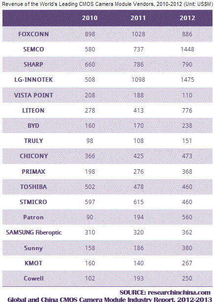
- CMOS sensor, optical lens, AFA, filter and module account for about 52%, 19%, 6%, 3% and 20% of the camera-module market size in 2012, respectively.
- The camera module industry market size in 2012 was approximately US$10.8B, an increase of 24.1% over 2011, mainly driven by the great improvement in smartphone camera pixels, which extended into 2013, whereupon the mainstream smartphone camera pixels will be raised from 5MP to 8MP, and the high-end smartphone as high as 13MP.
- In 2013 camera module market size is expected to climb 23.1% over 2012 to US$13.3 billion.
- In 2013, all smartphones will be equipped with AFA, and high-end ones given with the OIS.
- Omnivision did all it could do to catch up from the second half of 2012 by lowering prices to stimulate sales. The consequent substantial growth of 50% in shipment narrowly kept its dominant position in the field of non-digital camera CMOS image sensor, followed closely by Samsung and Sony.
Thursday, April 04, 2013
Imaging Forum Announcement
Albert Theuwissen announces the First Solid-State Imaging Forum to be held on Dec 16-17 in Amsterdam, Netherlands. The audience will be limited to 30 people to stimulate interaction between the participants and the speaker(s). The subject of the first forum will be "ADCs for Image Sensors". Only world-leading and independent expert(s) will be cont(r)acted to talk at the forum.
More information will follow in the coming weeks or months.
More information will follow in the coming weeks or months.
SiOnyx Announces First Products
PR Newswire: SiOnyx announces the XQE family of CMOS image sensors. XQE sensors are said to deliver "unprecedented performance advantages in infrared imaging with sensitivity enhancements as high as 10x incumbent solutions." The XQE family includes three sensors: the 10um pixel-based 1.3MP XQE-1310, and the 5.6um pixel-based 1.0MP XQE-0920 and 0.6MP XQE-0570. The XQE sensor family is based upon SiOnyx’ black silicon technology that enhances the sensitivity of silicon based light detectors. All sensors in the XQE family have ultra-low read noise and 72dB of native DR. Additionally, all XQE sensors have on-chip HDR features that allow up to 120dB dynamic range capability. XQE sensors are fabricated with a standard CMOS process that offers low power, low dark current, and no sensor cooling requirements.
"These new XQE sensors represent a tremendous accomplishment for our sensor team and our company," said Stephen Saylor, President and CEO of SiOnyx. "Since CCD and CMOS sensors were invented decades ago, image sensor development has focused almost entirely on capturing images in the visible spectrum. XQE sensors build upon this foundation of excellence and add a new dimension of extraordinarily high sensitivity in the near infrared spectrum."
IR sensitivity is important in many applications including biometrics, eye tracking, gesture recognition and surveillance. In surveillance, enhanced IR sensitivity takes advantage of the naturally occurring IR ‘nightglow’ to enable imaging under conditions that normally require very expensive image intensified night vision equipment.
"IR imaging is a fundamental enabler for any man-machine interface," said Dr. Homayoon Haddad, VP Engineering and CTO of SiOnyx. "Applications as diverse as autonomous vehicles and gaming depend on IR light to enable systems to measure, analyze, and adapt to the environment around them."
SiOnyx XQE image sensors are sampling in Q2 2013 to customers interested in evaluating the use of XQE image sensors in next generation imaging platforms.
 |
| XQE-1310 moonless night 1/30s f1.4 |
 |
| XQE-0570 full moon 1/30s f1.2 XQE-0920 exhibits similar night vision performance |

Pelican Imaging Uses AEi Active Alignment System
EON: Automation Engineering Incorporated (AEi) collaborates with Pelican Imaging to implement 6 degrees of freedom active alignment for computational array cameras using AEi's CMAT (Camera Module Align, Assembly, and Test) flexible automation platforms.
According to AEi CTO Andre By, "AEi has a successful history of implementing active optical alignment for various products for many years now, focusing on the manufacture of camera modules for the past several years. We are now introducing further enhancements to this technology to facilitate mass production of the Pelican multi image array style of cameras."
According to AEi CTO Andre By, "AEi has a successful history of implementing active optical alignment for various products for many years now, focusing on the manufacture of camera modules for the past several years. We are now introducing further enhancements to this technology to facilitate mass production of the Pelican multi image array style of cameras."
Wednesday, April 03, 2013
HTC "Ultrapixels" Made by ST
Chipworks reverse engineering team revealed that recently announced HTC Ultrapixels are in fact BSI pixels made by ST. The 4MP 2.0um pixel sensor is the first ST-manufactured BSI sensor that Chipworks has seen:
| HTC-ST Ultrapixel Sensor |
Tuesday, April 02, 2013
Xilinx Zynq-7000 Video and Imaging Kit
Xilinx published a Youtube video demo of its Zynq-7000-based ZC702 Video Processing Platform Evaluation Kit:
Subscribe to:
Posts (Atom)