Friday, November 30, 2012

IISW 2013 Final Call for Papers

2013 International Image Sensor Workshop (IISW), to be held on Snowbird Resort, Utah, USA, June 12-16, 2013, published a Final Call for Papers:

The scope of the workshop includes all aspects of electronic image sensor design and
development. In addition to regular papers, the workshop will include invited talks, poster presentations, discussion sessions, and Walter Kosonocky Award. Extra time has been added to permit longer discussion and more informal meeting time.

Papers on the following topics are solicited:

Image Sensor Design and Performance

  • CMOS Image sensors, CCD and CID image sensors. New architectures.
  • Image sensors with rolling shutter and global shutter.
  • Image sensors architecture, Low noise readout circuitry, ADC designs
  • High frame rate Image sensors, High dynamic range sensors, Low voltage and low power
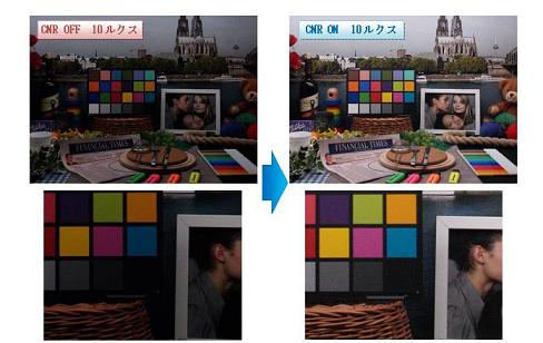
  • High image quality. Low noise. High sensitivity. High color reproduction.
  • Non-standard color patterns with special digital processing
  • System-on-a-chip, Image sensors with digital preprocessing

Pixels and Image Sensor Device Physics

  • New devices and structures. Advanced materials.
  • Small pixels development, testing, and characterization
  • New device physics and phenomena
  • Techniques for increasing QE, well capacity, reducing crosstalk, and improving angular performance
  • Front side illuminated and back side illuminated pixels and pixel arrays
  • Nanotechnologies for Imaging
  • Pixel simulation: Optical and Electrical simulation, 2D and 3D, CAD for design and simulation.

Application Specific Imagers

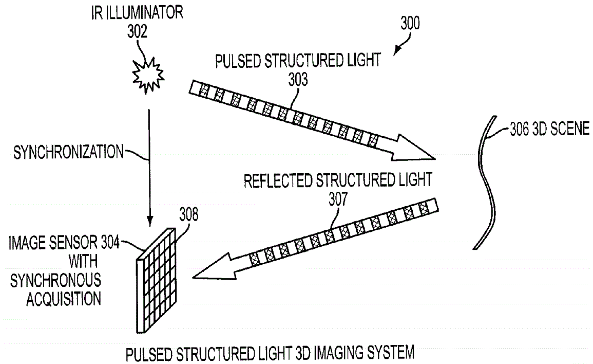
  • Image sensors and pixels for depth sensing: TOF, RGBZ, Structured light, etc.
  • Image sensors with enhanced spectral sensitivity (NIR, UV)
  • Pixels and Image sensors for stereo Imaging
  • Sensors for DVC, DSC, Mobile, DSLR and mirror-less cameras
  • Array Imagers and sensors for Computational Imaging
  • Sensors for medical applications, microbiology, genome sequencing,
  • High energy photon and particle sensors (X-ray, Radiation).

Fabrication and testing

  • New fabrication techniques. Backside thinning. Scaling.
  • Wafer stacking, multilayer sensors, “3D” integration
  • Advanced optical path, Color filters. Microlens. Light guide
  • Packaging and Testing. Wafer level cameras
  • Reliability. Yield. Cost.
  • Defects. Leakage current. Radiation damage.

Submission of papers: Abstracts should be submitted electronically to the Technical Program Chair, Gennadiy Agranov (see email in the pdf on IISW site). The deadline for abstracts submission is January 23, 2013.

8MP Stacked Sensor, 12MP Power and Speed Marvel and More From Sony

Sony Cx-News vol. 70 is entirely devoted to new and very impressive image sensor announcements. The first of the two most interesting ones is 1.55um BSI pixel-based IMX117CQT. This 1/2.3-inch 12.4MP sensor is an improvement on the similar but older IMX078CQK. The new sensor is faster, lower power, has wider light acceptance angle, and more:


The sensor is very fast delivering 35fps at full resolution at 430mW power. It also capable to 4K/60fps video (10b ADC mode) and includes HD-ish slow motion modes:


Another important announcement is the first stacked sensor product, the 1/4-inch 8MP 1.12um pixel ISX014, naturally, with integrated ISP:

Sony illustration of the stacked structure does not seem to have
any wafer-to-wafer contacts in the pixel array area

Not much information is given about the sensor. It supports 1940 x 1080p video at 30fps and 1280 x 720p video at 60fps. The built-in scalar function makes it possible to shrink all of the 8MP to perform 16:9 cropping for video. Power consumption is 270 mW in 8MP JPEG@15fps mode or 202 mW in 2MP YUV@30mode which are quite good numbers, possibly due to an advanced process node used for ISP die.

The image samples which were supposed to show the sensor's high quality, are of low resolution, unfortunately:


Another announcement is the new 1-inch 9.19MP CCDs: the ICX814ALG (B&W) and the ICX814AQG (color). The sensors have 4 outputs and multitude of readout modes, the fastest one being 1080p at 36fps:

Thursday, November 29, 2012

Raymond Wu Re-Joins Omnivision

PR Newswire: Omnivision reported its quarterly results on the higher end of its guidance: $390.1M, as compared to $258.1M in the previous quarter, and $217.9M a year ago. GAAP net income $10.3M, as compared to $2.3M in the previous quarter, and $21.1M a year ago.

GAAP gross margin is 16.6%, as compared to 19.1% in the previous quarter and 30.6% a year ago. The sequential decrease was attributed to an increase in shipment mix of advanced products that carried high manufacturing costs.

"In addition, I am pleased to announce the addition of Raymond Wu to OmniVision's management team," said Shaw Hong, Omnivision's CEO. "Raymond, one of our co-founders, has agreed to re-join us as our President, effective December 1, 2012. During his previous tenure, Raymond's intellect, experience and influence extended to market development, engineering and sales. We are enthused by his return, and with his knowledge of our company and the industry, I expect Raymond to make significant contributions to OmniVision's continued growth in the years to come."

Raymond Wu used to be Omnivision's EVP and left the company in August 2006.

Update: SeekingAlpha published Omnivision's earnings call transcript with more details on its business.

PMD and Mesa ToF Cameras Comparison

Open access Remote Sensing journal published a nice paper comparing PMD's CamCube3.0 and Mesa Imaging's SR-4000 ToF cameras and also giving a nice background on other ToF solutions:

SR-4000 and CamCube3.0 Time of Flight (ToF) Cameras: Tests and Comparison
Dario Piatti and Fulvio Rinaudo
DITAG, Politecnico di Torino, Torino, Italy

The paper starts with a nice table filled with parameters of many ToF cameras, both historical and available now on the market:


The influence of camera warm-up on distance measurement is analyzed: a warm-up of 40 minutes is suggested to obtain the measurement stability, especially in the case of the PMD's CamCube3.0. Depth accuracy tests have shown similar numbers of of order of millimeters for both cameras.

Mesa's SR-4000 is on the left, PMD's CamCube3.0 on the right.
Question mark means the accuracy has not been measured yet.

Via Vision Systems Design.

Pansonic Presents its SmartFSI at IDW 2012

International Display Workshops combined with Asia Display 2012 to be held in Kyoto, Japan on December 4-7, has few image sensor presentations. For the first time Panasonic openly presents its SmartFSI technology:

Evolution of Eyes and Image Sensors
H. Watanabe
Panasonic, Japan

The evolution of the eye and image sensors was overviewed. The possible disadvantage of the inverted structures of human eyes and FSI image sensors was solved with the use of the lightpipe function. A novel “SmartFSI” image sensor with stacked lightpipe structure demonstrated a high performance.

There are quite a few other interesting presentations, including 3 by Samsung:

A 1.5 Mpixel RGBZ CMOS Image Sensor for User Interface and 3D Image Capture
W. Kim, J. Yun, S.-H. Lee, Y. Wang, I. Ovsiannikov, Y. Park, C. Chung
Samsung, Korea, USA

A 1.5 Mpixel RGBZ image sensor to capture color (RGB) and depth (Z) at the same time is presented. Time-Of-Flight (TOF) method is used for depth. Color pixels and depth pixels are placed together in pixel array with specially designed RGBZ pattern. It demonstrates excellent depth performance and full color image.

A Full-HD CMOS Image Sensor with TimeMultiplexed 2D/3D Image Acquisition
S.-J. Kim, J. Shin, J. D. K. Kim, B. Kang, K. Lee
Samsung Advanced Inst. of Tech., Korea

We present a 1920x1080 pixel array to provide high-resolution 2D color images and high-accuracy 3D depth maps in a time-multiplexed manner. The prototype chip demonstrates the demodulation of 20 MHz time-of-flight signal with the contrast of 52.8%, achieving less than 38 mm depth error between the distance of 0.75 m and 4.5 m. [For a good multi-purpose gesture recognition one needs less than 10mm accuracy - ISW]

Amorphous Oxide Semiconductor Thin Film Transistor for Novel Device Applications
S. Jeon, I. Song, S.-E. Ahn, C. I. Kim, U.-I. Chung
Samsung Advanced Inst. of Tech., Samsung Elect., Korea

Among various semiconductor devices, electronically active oxide thin film transistors (TFTs) have received considerable attention for a wide range of device applications. In this presentation, we review various device applications utilizing amorphous oxide semiconductor TFT, which include photo-sensor, image sensor and other device applications.

Low Noise Readout Circuits Interface Using a Capacitive-Feedback Frontend Amplifier for High Output Impedance Sensors
K. Mars, S. Kawahito
Shizuoka Univ., Japan

In this paper a low-noise high-gain readout circuit interface for high output impedance sensors is presented. Theoretical noise analysis and simulation results shows that by using a high-gain switched capacitor amplifier, the thermal noise is greatly reduced if the dominant reset noise component at the charge summing node is canceled.

An Ultra-Low Voltage CMOS Imager with Novel Pulse-Width-Modulation Readout
C.-C. Hsieh, M.-T. Chung
Nat. Tsing Hua Univ., Taiwan

A 0.5 V PWM CMOS Imager chip with threshold variation cancelling and programmable threshold control scheme was implemented. It achieves 0.055% pixel FPN, 0.65 LSBrms random noise at dark, and 82 dB dynamic range at 11.8 fps. The chip consumes 4.95 µW at 11.8 fps; results in a iFOM as 163.9 pW/f-p.

Discussing Pixel Circuits for Hybrid Sensor and Display Pixel Arrays
N. Papadopoulos, M. Yang, M. Esmaeili-Rad, M. Sachdev, W. S. Wong
Univ. of Waterloo, Canada

The hybrid sensor and display pixel proposed consists of: light sensor and integrated display onto the backplane. Phototransistors incorporating both sensing and switching on the same device was used. The backplane was implemented using a driving TFT and an OLED. The grey scale is generated by pulse-height and width voltage modulation.

Report from Symposium on Microoptical Imaging and Projection, Part 3

Albert Theuwissen concludes his series of reports by the discussion of poLight AF technology presented at the Symposium.

More Leap and PMD Demos

Leap Motion added 4 more video demos to its third-party developers playlist, so that the list currently has 7 videos. Most of the new videos demo gesture control in games.

Meanwhile PMD too published the finger tracking demo running on its CamBoard nano platform:

Advantest Upgraded its CIS Tester Speed

Advantest introduces what it claims to be the industry's fastest image-capture module to cost-efficiently test image sensors with D-PHY and M-PHY interfaces. The new T2000 3Gbps CMOS Image Capture Module operates on its T2000 ISS system:


The T2000 3Gbps CMOS Image Capture Module simultaneously tests up to 64 devices in parallel, significantly reducing test costs. In addition to improving yields by performing at-speed testing in production, the module also can be used to shorten turnaround time in verifying semiconductor designs on first silicon.


"Ongoing, rapid improvements in the performance and resolution of CMOS image sensors as well as the growing volume of electronic products depending upon them continue to exert downward pressure on production costs," said Satoru Nagumo, senior vice president of the ASD Test Business Group at Advantest Corporation. "Our newest generation of image-capturing technology enables our customers to lower the cost of test while meeting the performance requirements for advanced image sensors."

Wednesday, November 28, 2012

Toshiba Announces 1.12um BSI Sensor with Improved SNR

PR Newswire: Toshiba announces a 13MP, 1.12um pixel sensor claimed to deliver high-image quality equivalent to a 1.4um pixel. The new T4K37 feature BSI and integrated color noise reduction (CNR) and fits into an 8.5mm x 8.5mm size camera module.

The miniaturization of pixel size impacts performance of light sensitivity and SNR in today's 1.12um pixel image sensors. BSI technology helps improve sensitivity, but is said to fall short on elevating image quality. Toshiba developed its newest image sensor with BSI and CNR integrated on the sensor to address both low-light sensitivity and SNR. As a result, the Toshiba CMOS image sensor provides approximately 1.5 times higher SNR than a 1.12um pixel sensor with no CNR.

Samples of the new Toshiba sensor, the T4K37, will be available in December 2012. Sample pricing begins at $20.00.


Update: It appears that Japanese PR has much more info. Among the pictures, it shows the CNR effect:


Here is the Google translation of CNR principle:

"CNR Our circuit has adopted the type to compare the image between frames by a digital filter circuit to suppress the color noise, without compromising a sense of resolution, of 1.12 micrometer pixel circuit not installed CNR SN ratio of about 1.5 times to accomplish, to achieve the SN ratio of the pixel corresponding to 1.4 micrometers."

The sensor is fast, it delivers 30fps at full 13MP resolution. The Japanese PR also has a table with two other sensors, apparently based on the same 1.12um pixel:


Update: Toshiba published a product page of the 1/3.07-inch T4K37 sensor. The block diagram shows a location of Color Noise Reduction part (CNR). The output format is either 8b or 10b.

Continuation of Report from Symposium on Microoptical Imaging and Projection

Albert Theuwissen continues his notes from the Fraunhofer Symposium in Jena, Germany. The second part covers Heptagon wafer level optics and a prototype multi-aperture camera, talks about Lytro news and technical details, Fraunhofer in-house CIS process, Nemotec wafer scale optics, ST pixel simulations, and more.

Tuesday, November 27, 2012

Report from Symposium on Microoptical Imaging and Projection

Albert Theuwissen published a first part of his report from Symposium on Microoptical Imaging and Projection being held these days in Fraunhofer Institute, Jena, Germany. The first part of the report talks about multi-aperture imaging presented by Pelican Imaging, LinX, Ascentia, Fraunhofer and Onera.

ON Semi and Teledyne Designed 16MP MCT Sensor

Business Wire: ON Semiconductor collaborated with Teledyne Imaging Sensors to manufacture an Extremely Large Stitched Read Out Integrated Circuit (ELS ROIC) for astronomy.

The 16MP H4RG-15 consists of Teledyne’s HgCdTe detector material hybridized to a CMOS readout circuit. It is said to be the largest sensor ever produced for IR astronomy. The H4RG-15 63 mm x 63 mm stitched CMOS ROIC uses ON Semiconductor’s proprietary 180nm process. The ROIC is so large that only four die fit onto a 200 mm wafer.

The H4RG-15 ROICs were manufactured at ON Semiconductor’s fab located in Gresham, Oregon. With this project, ON Semiconductor has demonstrated that it can successfully produce the H4RG-15 with the yield required for this next generation sensor.

The H4RG-15 sensor has been installed at the University of Hawaii’s observatory on Mauna Kea to confirm the performance of the sensor under telescope observing conditions. "The resolution with which images can be captured using this new sensor system represents a major step forward in the progression of IR astronomy," said Dr. Donald Hall of the Institute for Astronomy at the University of Hawaii, who is the principal investigator for the NSF-funded H4RG-15 development program.

Saturday, November 24, 2012

Samsung S5K3H5 CMOS Sensor Promo

Samsung published a Youtube promo of its 8MP, 1.4um pixel S5K3H5 sensor promo. The sensor is used in Samsung Galaxy S3 smartphone. The video goes through the sensor spec with the video illustrations in the background. Another feature of the video is the 1.9MP 1/6-inch 1.75um pixel front sensor S5K6A3:

Friday, November 23, 2012

Leap Motion's Demos on Youtube

There are few new Leap Motion's gesture control videos appeared on Youtube. The videos are from different third party developers that Leap Motion kindly collected into a single playlist.

The first one shows finger recognition in action. The room is quite dark, hopefully it's not a system limitation:


The Quadrotor control works quite nicely. A delay is noticeable but it might come from mechanical stuff:


The pong game gesture control is shown in dark room too:

Thursday, November 22, 2012

IS2013 Publishes Confirmed Speakers List

Image Sensors 2013 conference to be held on March 19-21, 2013 in London, UK, published an impressive list of confirmed speakers:
  • Dr Howard E Rhodes, CTO, OmniVision, USA
  • Prof Franco Zappa, PoliMI, Italy
  • Dr G Humpston, Director of Applications (Europe), Digital Optics Corporation, UK
  • Dr.Ir Peter Centen, Director R&D, BU Cameras Grass Valley, The Netherlands
  • Prof Edoardo Charbon, TU Delft, The Netherlands
  • Paul Danini, Technology & Market Analyst, Imaging Technologies & Mems Devices, Yole Developpement, France
  • Dietmar Wueller, Director, Image Engineering, Germany
  • Dr Gerhard Holst, Head of R&D, PCO, Germany

ST Proposes LDO Regulator with Distributed Output Stage

ST patent application US20120286135 "Low drop-out regulator with distributed output network" by Jingfeng Gong, Yann Desprez-Le-Goarant (Singapore), proposed a regulator for a pixel array with distributed output transistor that "improves localized heat dissipation by spatially-distributing transistors, and reduces IR drop across an output track by providing a consistent output voltage at each output node located along the output track." (I'd say with improved consistency, not exactly the same voltages).

The prior art is shown on Fig. 1A:


The proposed solution is shown on Fig. 2:

Wednesday, November 21, 2012

DALSA Wins Netherlands-Canadian Chamber of Commerce’s Business of the Year Award

Teledyne DALSA has been honored as Business of the Year by the Netherlands-Canadian Chamber of Commerce (NCCC). The NCCC’s annual award is presented to Canadian companies with a subsidiary in the Netherlands or to Dutch companies active in Canada.

The selection committee noted the success of Teledyne DALSA’s Netherlands-based Professional Imaging division. Located in the High Tech Campus in Eindhoven, which has been called “the smartest square kilometer in Europe” by Fortune magazine, the division developing large format image sensors and medical x-ray detectors.

"We are delighted and humbled to accept this honor," commented Dr. Edwin Roks, EVP and Managing Director of Teledyne DALSA’s Eindhoven operations. "None of our innovation happens in isolation. The collaboration between our groups in Canada and in The Netherlands is extremely important for us. I would like to thank the embassy and the NCCC for their role in facilitating transatlantic cooperation, and we will strive to continue this valuable, productive relationship."

Bryce Bayer Died

Imaging Resource: Bryce Bayer, the Eastman Kodak scientist who invented the almost standard color filter pattern that bears his name, has passed away. Bayer, 83, died on November 13th in Bath, Maine. The Bayer Filter array was patented in 1976, U.S. Patent No. 3,971,065. Bayer is also known for his recursively defined matrix used in ordered dithering.


Update: SR kindly sent me a photo of Bryce Bayer's notebook describing his RGB pattern idea for the first time:

Tuesday, November 20, 2012

Sharp Designs its Own CMOS Sensors

Sharp has been mostly known by its CCDs. The 2012 Sharp Components Catalog does not even mention CMOS sensors as a product category. However, one the the Oct. 2012 Cadence success stories reveals that "Recently Sharp embarked on designing a new consumer electronics CMOS image sensor."

"Cadence helped us achieve our target in the highly competitive arena of CMOS image sensors,” says Naoya Fujita, GM of Product Planning, Electronic Components and Devices Group, Sharp. "We were able to deliver the highest quality of silicon and get to market significantly faster than would have been possible with our previous flow. We exceeded our design requirements and expectations, and look forward to continued collaboration with Cadence to meet the growing demand for high-quality CMOS images sensors."

Monday, November 19, 2012

ASIC for Large Format NIR/SWIR Imager Project Started

EETimes: A consortium formed by the Caeleste, Belgium, Easics, Belgium and SELEX Galileo, UK won the European Space Agency's call for tender AO/1-6814 Development of Prototype ASIC for Large Format NIR/SWIR Detector Array. The ASIC is targeted for use in future Space Science and Earth Observation missions. The 18 month development aims to design an ASIC dedicated to large format cryogenic NIR/SWIR Detector. The project has several challenging features:

  • 77K operation temperature
  • Radiation hardness
  • Fully programmable sequencer on chip
  • 16bits analog to digital conversion chain

The project will benefit from the experience of each consortium partner. Caeleste is responsible for the project supervision and the design of the analog section. Easics is designing the digital section using IMEC standard DARE library for radiation hardness. Easics is also in charge of the test system development. SELEX Galileo joins as IR/cryogenic expert and will provide support for cryogenic operation, test and evaluation.

Following the successful completion of this demonstrator phase, an industrialized version will be envisaged, aiming at providing such flexible and standard ASIC to European Companies willing to simplify the design of infrared instruments for space application.


Thanks to BD for sending me the news!

Image Sensors at ISSCC 2013

ISSCC 2013 published its advance program with many image sensor papers, including Sony stacked sensor presentation:

A 1/4-inch 8Mpixel Back-Illuminated Stacked CMOS Image Sensor
S. Sukegawa, T. Umebayashi, T. Nakajima, H. Kawanobe, K. Koseki, I. Hirota, T. Haruta, M. Kasai, K. Fukumoto, T. Wakano, K. Inoue, H. Takahashi, T. Nagano, Y. Nitta, T. Hirayama, N. Fukushima
Sony, Atsugi, Japan;
Sony LSI Design, Atsugi, Japan
Sony Semiconductor, Kumamoto, Japan

A 3.4µW CMOS Image Sensor with Embedded Feature-Extraction Algorithm for Motion-Triggered Object-of-Interest Imaging
J. Choi, S. Park, J. Cho, E. Yoon, University of Michigan, Ann Arbor, MI

A 467nW CMOS Visual Motion Sensor with Temporal Averaging and Pixel Aggregation
G. Kim, M. Barangi, Z. Foo, N. Pinckney, S. Bang, D. Blaauw, D. Sylvester University of Michigan, Ann Arbor, MI

A Rolling-Shutter Distortion-Free 3D Stacked Image Sensor with -160dB Parasitic Light Sensitivity In-Pixel Storage Node
J. Aoki, Y. Takemoto, K. Kobayashi, N. Sakaguchi, M. Tsukimura, N. Takazawa, H. Kato, T. Kondo, H. Saito, Y. Gomi, Y. Tadaki, Olympus, Hachioji, Japan

An 8×16-pixel 92kSPAD Time-Resolved Sensor with On-Pixel 64ps 12b TDC and 100MS/s Real-Time Energy Histogramming in 0.13µm CIS Technology for PET/MRI Applications
L. H. Braga, L. Gasparini, L. Grant, R. K. Henderson, N. Massari, M. Perenzoni, D. Stoppa, R. Walker
Fondazione Bruno Kessler, Trento, Italy
STMicroelectronics, Edinburgh, UK
University of Edinburgh, Edinburgh, UK

A 0.18µm CMOS SoC for a 100m-Range 10fps 200×96-Pixel Time-of-Flight Depth Sensor
C. Niclass, M. Soga, H. Matsubara, M. Ogawa, M. Kagami
Toyota Central R&D Labs, Nagakute, Japan

3D Camera Based on Linear-Mode Gain-Modulated Avalanche Photodiodes
O. Shcherbakova, L. Pancheri, G-F. Dalla Betta, N. Massari, D. Stoppa
University of Trento, Trento, Italy.
Fondazione Bruno Kessler, Trento, Italy

A 3D Vision 2.1Mpixel Image Sensor for Single-Lens Camera Systems
S. Koyama, K. Onozawa, K. Tanaka, Y. Kato
Panasonic, Nagaokakyo, Japan

A 187.5µVrms-Read-Noise 51mW 1.4Mpixel CMOS Image Sensor with PMOSCAP Column CDS and 10b Self-Differential Offset-Cancelled Pipeline SAR-ADC
J. Deguchi, F. Tachibana, M. Morimoto, M. Chiba, T. Miyaba, H. Tanaka, K. Takenaka, S. Funayama, K. Amano, K. Sugiura, R. Okamoto, S. Kousai
Toshiba, Kawasaki, Japan;
Toshiba Microelectronics, Kawasaki, Japan

A 94GHz 3D-Image Radar Engine with 4TX/4RX Beamforming Scan Technique in 65nm CMOS
P-N. Chen, P-J. Peng, C. Kao, Y-L. Chen, J. Lee
National Taiwan University, Taipei, Taiwan

A [10°C ; 70°C] 640×480 17µm Pixel Pitch TEC-Less IR Bolometer Imager with Below 50mK and Below 4V Power Supply
B. Dupont, A. Dupret, S. Becker, A. Hamelin, F. Guellec, P. Imperinetti, W. Rabaud
CEA-LETI-MINATEC, Grenoble, France

The conference's forums include F4 Scientific Imaging forum having few nice overview presentations:

Overview of Scientific Imaging in the Frequency Range from X-Rays to Terahertz
Valérie Nguyen, CEA Leti MINATEC, Grenoble, France

Multispectral Imaging: When CMOS Does the Trick!
Matteo Perenzoni, Fondazione Bruno Kessler, Torento, Italy

Ultra-High-Speed Imaging
Shigetoshi Sugawa, Tohoku University, Sendai, Japan

Single-Photon Imaging with SPADs
Robert Henderson, University of Edinburgh, Edinburgh, UK

State-of-the-Art in Uncooled IR Sensors and Readout Circuitry
Patrick Robert, ULIS, Veurey-Voroize, France

High-Sensitivity Astronomical-Imaging Arrays with Cryogenic Electronics for Terahertz Waves
Hiroshi Matsuo, National Observatory of Japan, Tokyo, Japan

THz Imaging: What You See and What You Don’t!
Peter H. Siegel, Caltech/JPL, Pasedena, CA

Advanced Microwave Imaging Based on Modern Semiconductor Technologies
Sherif-Sayed Ahmed, Rohde & Schwarz, Munich, Germany

THz CMOS Image Sensors Using Schottky Barrier Diodes for Lensless Portable Applications
Kenneth O, University of Texas at Dallas, Dallas, TX

Sunday, November 18, 2012

Pelican Imaging Capabilities Presented

Pelican Imaging starts to present its approach at different forums. Apparently, Mobiletrax' post is based on one of those presentations:

"The founders of Pelican Imaging started with the idea of using an array of low resolution photoplanes coupled to an array of small lenses and using the overlapping information to create astounding images and videos.

The core intellectual property (IP) starts by using an array of 16 inexpensive, mass produced accurately aligned cameras. The array creates 16 images – each one slightly different from the other since it is capturing the image from a slightly different angle. Because the input images all come from lenses and pixel technologies that are mature and low cost, the yield of the solution should be very good. You can see the 16 ‘similar’ images captured by using the 16 lenses in Figure 2.
"


"Because each image is taken from a slightly different angle, the processing logic can determine the distance objects are from the camera, thus providing a depth map of the scene... And, the 16 slightly different versions of the photo offer the ability for Pelican’s proprietary (and patent pending) software to synthesize a higher resolution image."

Some of the camera capabilities are shown in pictures:

Saturday, November 17, 2012

Aptina Applies for Patent on Structured Light Sensor with Background Subtraction

Aptina's patent applications US20120274744 and EP2519001 "Structured light imaging system" by Chung Chyn Wan, Xiangli Li and Gennadiy Agranov proposes background light extraction in stuctured light system with pulsed light source:


The signal plus background and background are stored on the different caps in the pixel...


...and then read out for further processing:

Friday, November 16, 2012

TSMC Applies for Entrenched Color Filters Patent

TSMC patent application US20120280346 "Sensor structure for optical performance enhancement" by Jhy-Ming Hung, Jen-Cheng Liu, Dun-Nian Yaung and Chun-Chieh Chuang proposes placing FSI color filters in trenches, similar to what ST and Samsung presented some time ago. The 140a,b,c are the color filters in trenches between the metal routing 126:

NIT Wins VISION 2012 Award

New Imaging Technologies MAGIC 3D solution has been chosen as the winner of the VISION Award 2012 by the jury. The new MAGIC 3D solution offers HDR stereo vision capability.

Recent FPGA Imaging News

Xilinx is aiming its Zynq-7000 "programmable SoC" platform to imaging and video applications, among other things:


EETimes and XCell Journal articles by Xilinx engineers talks about implementation of digital camera pipeline in general and white balance algorithms with more specifics (don't expect big revelations there):


PRNewswire: Meanwhile, Altera presented its FPGA-based automotive rear view camera, forward looking stereo camera, and radar/camera fusion systems.

Marketwire: Lattice and New Imaging Technology presented HDR camera based on NIT NSC1005 and LatticeECP3 FPGA.

Update: Xilinx published its FPGA reference design documentation based on ON Semi VITA-2000 image sensor.

Thursday, November 15, 2012

3 Ways to Measure Conversion Gain

Albert Theuwissen describes three ways to measure conversion gain. Some of them are well known, others less so. Educating read!

Wednesday, November 14, 2012

Sony Issues Convertible Bonds to Fund Image Sensors Capacity Expansion

Benzinga: Sony announces that it is planning to issue a 150 billion yen ($1.9 billion) zero coupon convertible bond maturing in 2017. The 60 billion yen ($750 million) is slated for the expansion of Sony's CMOS sensor production facilities in Nagasaki (announced on June 22, 2012, with an expected total capital expenditure of approximately 80 billion yen, expected to be completed during the first half of the fiscal year ending March 31, 2014).

Tessera/DOC Cuts EDoF Development, Concentrates on MEMS Motors

Business Wire: Tessera announces its wholly owned subsidiary, DigitalOptics Corporation ("DOC") will focus its efforts on its core MEMS camera module business. DOC plans to reduce its workforce – not including those related to manufacturing operations in Zhuhai, China – by up to 40%.

As part of this process DOC plans to cease operations at its facility in Tel Aviv, Israel and to pursue a possible sale of, or other strategic alternatives for, its facility in Charlotte, North Carolina. These two facilities are not central to the MEMS camera module opportunity. Given full effect, the planned actions would reduce the non-Zhuhai workforce of 450 by approximately 180 employees.

DOC anticipates that the staff reductions and facility dispositions will be spread over the next two to three quarters to ensure continuity in the business as well as compliance with relevant legal requirements.

Tel Aviv facility was developing EDoF, OptiML Zoom, OptiML Low-Light and other computational optics technologies. It was based on two acquired startups - Eyesquad and Dblur, combined with few people left from Shellcase. A number of key people of this group left Tessera a year ago, in Aug. 2011.

"Camera module features and functions have increasing importance to consumers in the mobile phone market. The changes announced today will focus DOC on that market and are an important part of driving the business towards profitability," said Robert A. Young, president and CEO of Tessera.

Omnivision's Shareholder Presentation

Omnivision's annual shareholder presentation from Sept. 27, 2012 has TSR-based market share data:


The company unit sales trend in the recent years is non-monotonic but still quite nice:

Tuesday, November 13, 2012

SQUIGGLE AF Motors in Giga-Pixel AWARE Camera

New Scale Technologies’ M3 focus modules have been designed into the next-generation AWARE cameras, the Duke University's gigapixel cameras assembled from many 14MP Aptina sensors.

The custom module with SQUIGGLE piezoelectric motor has a cross section less than 6 X 10 mm, a stroke of 2.5 mm and resolution of 0.5um. It moves a lens weighing several grams, so that each of the hundreds lenses can adjust its focus independently.

New Scale Technologies' custom M3 micro-mechatronics module

e2v Features in Electronics Weekly

The best image sensors come from Essex, UK, or so Electronics Weekly says. "Most of the image sensors in space or in ground-based astronomy are made here in Chelmsford," John Kemp, marketing and applications manager at e2v tells to the newspaper. Spacecraft Kepler, Solar Dynamics Observatory, NASA’s Curiosity Mars rover, Hubble space telescope, 1 Gigapixel Gaia camera, all use e2v sensors.

The company’s flagship CCD sensors are made in Chelmsford, Essex, UK on a bulk/epitaxial 6-inch process whose details are the result of 20 years of experience, and remain confidential. The CMOS sensors are made on outside fabs.

Monday, November 12, 2012

Aptina Announces Automotive HDR ISPs

Business Wire: Aptina introduces the AP0100AT and AP0101AT, two dedicated automotive image co-processors supportion the company's HDR sensors. The two-chip solution of sensor and co-processor allows for multiple camera price and performance points with re-use of circuit board design, fast time to market and design flexibility. Sensor performance is enhanced by the reduction in heat resulting from a separate co-processor chip while at the same time enabling high performance features.

Both co-processors provide color processing, AWB and AE support, noise reduction, and Adaptive Local Tone Mapping (ALTM) to enhance HDR display. The AP0101AT is aimed to Automotive Digital Surround View Systems, supporting 1.2MP video at 45fps and 720p video at 60 fps, and consumes 129mW. The AP0100AT supports 185-degree fisheye lens distortion correction, perspective correction and multiple view options such as split side view, triptych and trailer hitch. In addition, AT0100AT has overlay capabilities and integrated NTSC/PAL encoder and consumes 170mW.

Currently, Aptina’s family of HDR megapixel automotive sensors includes the 1/3”-optical format, AR0132AT. Other sensors will be announced as they become available, including a ¼”-optical format 1.2-megapixel sensor, and a 1/5”-optical format WVGA sensor.

The AP0101AT is available now in a 6.5mm x 6.5mm VFBGA package with 0.65mm ball pitch, and the AP0100AT will be available in Q1 of 2013. Both products are AEC-Q100 qualified.

Sunday, November 11, 2012

EMVA 1288 Matures Up to V3.1

European Machine Vision Association is about to update its famous image sensors and cameras characterization standard to version 3.1. The published EMVA 1288 release candidate contains only a few refinements and additions to release 3.0, as listed in appendix D. The major additions are: total SNR curve including the spatial inhomogeneities in the double-logarithmic SNR plot, plots of horizontal and vertical profiles for illustration of the spatial inhonogeneities and the design of a template data sheet. The template defines QE, SNR and PTC plots.

If there are no objections against the new release, it will become final and will replace release 3.0 on January, 14, 2013.

Saturday, November 10, 2012

Raytrix Presents its Technology

Raytrix published its presentation at Nvidia GPU Technology Conference held in May 2012 in San Jose, CA. The 38min-long video explains the technology behind its light field camera:


The video is mostly based on the company's technology presentation from 2011. By that time the lightfield cameras competitive landscape looked like that (note, Lytro was not in production yet):


The latest Raytrix R11 camera has an array of about 20,000 microlenses, produces 2.7MP images out of 11MP sensor and uses a fast Nvidia GeForce GTX 580 card to deliver 30fps video. The camera costs 20,000 euros.

A nice overview of light field cameras was published by IEEE Spectrum in May 2012.

Friday, November 09, 2012

Step by Step poLight Approaches Mass Production

i-Micronews published an interview with François Vieillard, poLight VP Marketing
& Sales. The company is planning to start volume production in Q1 next year, fabbing the MEMS actuator at Texas Instruments and assembling the lens unit at a major electronics assembly house in Asia. Multiple camera module customers in Japan,
Korea and Taiwan will then need several months to qualify their modules with the unit, and then phone makers will need another few months to qualify the modules in their phones.

Himax Reports CIS Sales Down, Wafer Optics Sales and Prospects Up

Himax reports its Q3 2012 results. The company CEO Jordan Wu updates on image sensor business status:

"In our CMOS image sensor product line, the delay of Win 8 launch from Q3 to Q4 affected our shipments of 1 mega-pixel sensor during the third quarter. However, we expect such demands to resume starting Q4 thanks to our design-wins with a number of tier-one laptop names. Beyond laptop, we have also won design-wins in smartphone, tablet and surveillance applications from a wide range of customers. We also launched a 5 mega-pixel sensor in the third quarter which targets smartphone market. It will begin some shipment in the fourth quarter.

Our wafer level optics experienced double digit growth during the third quarter. The production of WLO for VGA, or 300,000-pixel, lens in our fab has been made smoothly with high and stable yields. With that, we are moving up the scale to start sampling our WLO with HD, or 1 mega-pixel, resolution, which we believe has a good potential of taking up a meaningful amount of the front camera market for smartphone. We expect our HD WLO to start mass production in early next year.
"

Thursday, November 08, 2012

Sony IMX128 Inside Nikon D600 DSLR

Chipworks published nice pictures of Nikon D600 internals featuring Sony 24MP, 5.9um pixel IMX128 sensor. From M1-level SEM photo, it looks like Sony uses 4-way shared pixel or 2-way sharing with mirrored layout:


Other than the main sensor, Chipworks analyzed the secondary AF assist sensor which also features what Nikon calls "Scene Recognition System" for evaluating "situation, brightness and color". Chipworks photo reveals non-Bayer color pattern on this sensor:

Aptina to Use Micron's 12-inch Fab

Up to now Aptina has used 8-inch Micron fabs. Generally, 8-inch wafer tools do not support processes beyond 90nm. According to Farshid Sabet, VP and GM of Mobile Division at Aptina, the company plans to produce its next-generation BSI sensors on Micron's 12-inch fab (Digitimes). Earlier, there were indirect indications that Aptina is going to use 12-inch TSMC process.

Other points from Farshid Sabet interview to Digitimes:

  • The mobile imaging market is trending toward emphasizing on image processing capability
  • This emerging trend will bring more opportunities for Aptina
  • The move by smartphone brands including Apple and HTC to reduce their reliance on component purchases from Samsung will also benefit Aptina
  • Aptina has been the only non-Japan-based CIS vendor that has managed to enter the supply chain of camera makers in Japan

Pixart Sees Mixed Sales Trends

Digitimes: Pixart is set to post sales growth of up to 5% sequentially in Q4 2012, according to company chairman Huang Sen-huang. Pixart boost in shipments of its optical mouse chips. However, it will be offset by a decrease in shipments of its games console solutions.

Pixart reported net profits of NT$120 million (US$4.1 million) on revenues of NT$970 million for Q3 2012.

Wednesday, November 07, 2012

Panavision Announces 17.4MP/90fps Global Shutter Sensor

Panavision Imaging announced the launch of its latest Dynamax 17.4MP CMOS image sensor (DYN0174) based on its Active Column Sensor (ACS) Technology. The new sensor features:

  • 14-bit per Column Distributed A/D- D/AD
  • Correlated Multi-Sampling- CMS
  • 4812 x 3624 Pixel Array
  • 5.0um pixel - Global/Rolling Shutter
  • >90FPS @ 4800 x 3600 (10-bit), >120FPS w/ROI
  • 2 Gigapixels/sec throughput
  • On-chip 125dB HDR in rolling shutter mode
  • As low as 5e- noise
  • 3 or 6 LVDS lanes
  • 14 bit Single Data Rate (SDR) per port can be folded to 7 bit Dual Data Date (DDR) to save pins

"Panavision Imaging is pleased to offer another high performance CMOS image sensor for industrial imaging applications", said Derrick Boston, President and CEO of Panavision Imaging.

This is the third area sensor to be launched in PVI’s family of Dynamax sensors, joining the 3.2MP sensor (DYN0032) and HDTV 2.1MP (DYN0021) which are already in the market.

Dynamax 17.4MP test samples have been released to various customers for their different market applications. The engineering grade devices will be available in a CPGA package by the end of 2012, in either color or monochrome versions. High volume production is planned in the middle of 2013.

PMD, Bluetechnix Announce 160fps ToF Camera

PMD´s partner Bluetechnix presents 3D ToF camera equipped with PMD PhotonICs 19k-S3 TOF 3D chip. The Argos3D-P100 camera captures depth picture at a resolution of 160x120 pixels with up to 160fps speed - claimed to be the highest framerate available for ToF cameras.

ST Settled Caltech Patent Infringement Claims

Law360.com: ST has settled claims brought by Caltech alleging STMicro, Nokia and RIM infringed image sensing technology patents.

Administrative Law Judge issued an order Monday putting the proceedings on hold pending the end of an ITC investigation and said the settlement would resolve claims that STMicro made smartphone camera components that allegedly infringed Caltech's patents and sold the parts to Nokia and RIM. "Caltech has entered into a settlement and license agreement with [STMicro] that resolves all outstanding issues in this investigation," the judge said.

The original lawsuit also included Siliconfile, SETi, Toshiba, LG and Pantech. Law360 article says that by now Caltech has settled with all defendants in that suit. The patents-in-suit are U.S. Patents 5,841,126; 5,990,506; and 6,606,122.

VISION 2012 Show Report

Albert Theuwissen published a nice report from VISION 2012 Show being held these days in Stuttgart, Germany. A lot of interesting stuff there: 16MP two-dimensionally curved sensor from Andanta, full-frame 35mm sensor by CMOSIS, global shutter HDR sensor by NIT and more.

Tuesday, November 06, 2012

More Market Views from Yole

As materials from Yole Developpement report "Status of the CMOS Image Sensors Industry" continue to trickle down, one more statement caught my attention:

"As volumes increase, a clear duality appears between companies that have adopted a growth strategy by focusing on low-end markets and those opting for a specialization in high-end and higher margin markets to maintain profitability such as STMicro and Aptina."


Regarding the hidden Y-axis scale, one can estimate it from the previously published data here.

P.S. Galaxycore's CAGR looks like much bigger than the stated 16%.

Monday, November 05, 2012

New iPads Rely on Omnivision's Sensors

Chipworks' iPad 4 teardown reveals two Omnivision sensors inside: the 5MP primary one with markings OV290BA and the 1.2MP secondary one with markings OV23CB.

Apple iPad mini too uses Omnivision sensors: the 5 MP primary camera has the same markings as Chipworks saw in the 5th generation iPod touch while the 1.2MP secondary camera is identical to that seen in the iPad 4.

Update: EETimes: UBM Techinsights confirms Chipworks' iPad 4 findings.

Omnivision Announces 5MP 1.75um OmniBSI+ Pixel Sensor

PR Newswire: OmniVision announces the OV5656, a cost-effective 5MP CameraChip sensor for smartphone, tablet and digital video camera (DVC) markets. The 1/3.2-inch OV5656 features 1.75um OmniBSI+ pixel with 1200mV/(lux*sec) sensitivity and delivers 30fps at full-resolution.

"Industry reports are predicting an annual demand of more than 450 million 5-megapixel image sensors over the next three years, and the OV5656's high performance and competitive cost structure make it a highly desirable camera solution for OEMs across multiple markets," said Vinoo Margasahayam, senior product marketing manager at OmniVision. "Compared to the previous-generation OV5650, the OV5656 delivers several performance improvements, including full resolution, high-speed 5-megapixel photography at 30 FPS, a 28 percent improvement in full-well capacity and significantly improved dynamic range in a smaller die size."

The sensor's integrated scaler allows it to record 1080p HD video at 30fps with electronic image stabilization (EIS) while maintaining full field-of-view (FOV). Using 2 x 2 binning functionality with post-binning re-sampling filter, the OV5656 can capture 720p HD video at 60fps. The OV5656 has 4-lane, 840Mbps/lane MIPI interface and LVDS serial output. The sensor's power consumption is 339mW.

The OV5656 fits into a module size of 8.5 x 8.5 with a z-height of less than 6 mm. It is currently available for sampling in both RW and CSP.

TowerJazz Showcases its CIS Solutions for Machine Vision

PR Newswire: TowerJazz is going to show its CIS customers products at VISION Show 2012 on November 6-8, 2012 in Stuttgart, Germany. The demonstrations will include: ON Semiconductor's VITA industrial image sensors, e2v Ruby sensors, the CMOSIS CMV family, the AnaFocus LINCE5M sensor, the Viimagic industrial sensor series, and the Truesense Imaging Inc. industrial CMOS sensor. Among TowerJazz's R&D partners in the show are: CSEM, Fraunhofer, and STFC.

TowerJazz is a provider of a wide range of pixel IP and an experienced R&D team that supports complex joint development projects. TowerJazz's 0.11um pixel design rule has been released for early adopters' designs. First product samples of this new platform were already delivered.

"TowerJazz is the only foundry exhibiting at VISION and we aim to establish our technology leadership and reinforce our relationships with existing customers as well as showcase our unique CMOS image sensor technology to make our offering more familiar to the end user," said Dr. Avi Strum, VP and GM, CIS Business Unit. "We are looking forward to participating at VISION to share our unique technology offering with attendees and connect with our image sensor partners to continue addressing our customers' growing needs."

"The industrial camera market is expected to grow steadily and to top $600M by 2016. Among the machine vision applications, intelligent traffic systems are experiencing very high growth," says Paul Danini, Technology and Market Analyst, Imaging Technologies & MEMS Devices, Yole Developpement.

Sunday, November 04, 2012

Next Generation TV Interface Technologies

Digitimes Research published a nice map of interface technologies battling for the next generation TV control:


Some of these technologies are based on sensors and optics. Primesense uses structured light 3D camera. Softkinetic and PMD use ToF cameras. Philips relies on IR triangulation for its motion sensing remote.

Saturday, November 03, 2012

Truesense Reports SNR10 of 7 lux for its 12MP CMOS Sensor

Keith Wetzel, a member of Truesense Imaging business development group, twitted that the new 12MP 4.7um pixel KAC-12040 CMOS image sensor "has an SNR10 value of ~7 lux." The lens aperture is not specified.

Sony Reports Higher Image Sensor Sales but Lowers Forecast

Slide 11 of Sony Q2 FY2012 earnings presentation says that "sales of ... image sensors are expected to be lower than previously anticipated, segment sales are expected to be lower than the August forecast". No reason for the forecast reduction is given.

Seeking Alpha earnings call transcript quotes Yoshinori Hashitani, Sony VP Investor Relations, saying that last quarter "sales of the image sensors increased because of strong demand of smartphones and other products".

Friday, November 02, 2012

High Speed Imaging Circa 1980

This Youtube video teardown shows internal design of Kodak Spin Physics high-speed digital camera, originally released in 1980. The camera had a resolution of 240x192 and frame rate of 2000fps - quite impressive numbers for a 30+ year old technology based on 34um pixels:


Here is the sensor's corner snapshot from the video:

Altasens Talks about Stacked Sensor Advantages

Altasens' patent application US20120267511 "Image sensor with hybrid heterostructure" by Lester Kozlowski has few interesting claims:

First, a stacked sensor structure is proposed:


The pixel array uses "optimized" pmos transistors. An example pixel capable of GS, S&H and CDS is shown on Fig. 6:


The main advantages of the stacked structure are (1) very good global shutter efficiency and (2) lower noise due to a special pmos transistor "optimization":

"FIGS. 7 and 8 [not shown here] compare the read noise achievable with optimized PMOS technology vs. standard CMOS technology wherein the source follower is formed in NMOS having flicker noise lower than readily achieved in common foundry processes, i.e., very good compared to what is readily available. Even so, the PMOS global shutter can yield a read noise of 1 e− (or holes) at a sense capacitance of 5 fF. The NMOS global shutter circuit instead has read noise of 3.5 e− at 5.5 fF. More importantly for long term development, the PMOS solution goes well below 1 e−0 as the sense capacitance is reduced while the NMOS solution plateaus well above 2 e−."

Toshiba Announces 8MP 1/3.2-inch BSI Sensor

Toshiba published a product page of 8MP 1.4um BSI pixel-based T4K34 sensor. The sensor did not appear on the previously published Toshiba roadmap. The new sensor is quite fast, delivering 30fps at full resolution and the same frame rate in 1080p mode. Its ADC resolution is selectable between 8b or 10b.

Thursday, November 01, 2012

Digital Camera Sensors Database

The new Digital Camera Database has an information on pixel size, sensor areas and more from 3281 digital cameras. The information is nicely presented in graphical and numerical form. It's hard to believe that the whole web site is just one-man job!

Thanks to GB for the link!

Kasalis Announces Pixid 300 Pro Availability

Kasalis announces the release of its Pixid 300 line of fully automated camera module assembly and test systems, featuring its active alignment technology. The Pixid 300 Pro and Pixid 300 Test models are now available for shipment.

"The increasing demands for improved image quality in mobile cameras has transformed the camera module industry, which now needs a cost-effective solution to meet the higher level of precision required in the alignment process," said Justin Roe, president of Kasalis. "The Pixid 300 Pro is a clear breakthrough that is changing the cost-benefit equation of active alignment for the whole industry. We have created a disruptive technology – the Pixid 300 Pro performs pre-dispense tests, adhesive dispense, dispense verification, active alignment, UV cure, and post-alignment tests all within 15 seconds, with a throughput of over 240 units per hour, and all for very competitive pricing."

The Pixid 300 Pro model is a fully automated manufacturing system featuring active alignment, customizable optical testing options, Adaptive Intelligence SPC, and automated adhesive dispense and UV cure. Each stage of assembly is performed in parallel to obtain the fastest possible throughput time. Adaptive Intelligence is a software suite that is embedded in the Pixid systems and improves the alignment process by using the machine feedback to improve its algorithms, thereby attaining faster speeds and improved yields. In addition to the Pixid 300 Pro, the series includes the Pixid 300 Test model, which is intended purely for the automated functional testing of camera modules.

The Pixid 300 series systems are designed for high volume production of camera modules such as those used in smartphones, automotive applications, webcams, medical imaging, and security cameras. Kasalis has designed all of the Pixid systems to solve industry challenges, provide easy upgrading and maintenance through modular parts, and to align a camera lens to a sensor in up to six degrees of freedom to obtain the best possible focus quality across the entire image sensor. As technology in mobile electronics advances, camera modules assembled with precision alignment are increasingly important.

Pixid 300 Pro

Workshop on Radiation Effects in Optoelectronic Detectors

2nd Workshop on Radiation Effects in Optoelectronic Detectors is to be held on November 28-29, 2012 in Toulouse, France, co-organised by CNES, ASTRIUM, THALES ALENIA SPACE, SODERN, ISAE. The program has papers devoted to radiation damage in CCD and CMOS senosrs:

Investigations on performance of Electron Multiplied CCD detectors (EMCCDs) after radiation for observation of low light star-like objects in scientific space missions
H. Michaelis, T. Behnke, S. Mottola, A. Krimlowski, German Aerospace Center, DLR, Institute of Planetary Research, Berlin (Germany), A. Holland, XCAM Ltd, Northampton, (UK), M. Schmid, Ingenieurbüro Schmid, Berlin (Germany)

The GAIA Radiation test campaigns: an historical review
D. Marchais, ASTRIUM SAS

A Comparison of Radiation Damage in CCDs From a Number of Flight Programmes
P. Jerram, E2V technologies

In-Orbit Results from CNES Satellite CCDs
A. Bardoux, A. Penquer, O. Gilard, R. Ecoffet, CNES, M. Auvergne, LESIA

Response of 3T and 4T Multi-Variant CMOS Image Sensors to Proton Radiation
A. Pike, J. Pratlong E2V Technologies

New Radiation Test Results on HAS2 CMOS Image Sensor
D. Hervé, M. Beaumel, SODERN, D. Van Aken, ON Semiconductor

Dark current degradation of a 5T 0.18µm e2v CMOS image sensor under gamma and proton irradiation
T. Nuns, J.P. David, ONERA, E. Martin, O. Gilard, CNES

CMOS monolithic sensors for vertex detector applications: TID effects and bulk damage study
L. Ratti, S. Zucca, Università di Pavia and INFN Pavia, L. Gaioni, INFN Pavia, G. Traversi, Università di Bergamo and INFN Pavia, S. Bettarini, G. Rizzo, Università di Pisa and INFN Pisa, F. Morsani, INFN Pisa, L. Bosisio, I. Rashevskaya, Università di Trieste and INFN Trieste

Radiation Effects in CMOS Image Sensor Isolation Oxides: Differences and Similarities with Thermal Oxides
M. Gaillardin, C. Marcandella, M. Martinez, P. Paillet, S. Girard, CEA DAM DIF, V. Goiffon, P. Magnan, M. Estribeau, ISAE, Image Sensor Research Team

Radiation Effects on Pinned Photodiode CMOS Image Sensors: Overview of Pixel Performance Degradation Due to Total Ionizing Dose
V. Goiffon, M. Estribeau, O. Marcelot, P.Cervantes, P. Magnan, P. Martin-Gonthier, R. Molina, F. Corbière, ISAE, Image Sensor Research Team, M. Gaillardin, S. Girard, P. Paillet,C. Marcandella, CEA DAM DIF, C. Virmontois, (Formerly at ISAE, now at CNES)

Recent radiation testing on 180 nm and 110 nm CMOS Image Sensor processes
J. Bogaerts, K. Van Wichelen, E. Gillisjans, G. Lepage, G. Meynants, CMOSIS nv

Displacement Damage Effects on Pinned Photodiode CIS
C. Virmontois, A. Bardoux, CNES, V. Goiffon, P. Magnan, F. Corbière, ISAE, Image Sensor Research Team, S. Girard, CEA DAM DIF

Single Event Effects in CMOS Image Sensors
V. Lalucaa, V. Goiffon, P. Magnan, ISAE, Image Sensor Research Team, G. Rolland, S. Petit, CNES

Vulnerability of CMOS image sensors in megajoule class laser harsh environment
P. Paillet, S. Girard, O. Duhamel, J.-L. Bourgade, S. Darbon, A. Rousseau, CEA, DAM, DIF, V. Goiffon, A. Chabane, P. Magnan, P. Cervantes, P. Martin-Gonthier, M. Estribeau, ISAE, Image Sensor Research Team, J. Baggio, CEA CESTA, V. Yu. Glebov, G. Pien, and T. C. Sangster, LLE, University of Rochester

Development of radiation tolerant EUV detectors and hybrid imagers
P. de Moor, IMEC

Specific tools developed for radiation tests at cryogenic temperature
A. Le Paih, F. Perrier, SOFRADIR

Radiation results on cooled infrared detectors
F. Perrier, A. Le Paih, SOFRADIR

Radiation testing of the MSI and Proba-V linear arrays
J. Vermeiren, Xenics

Evaluation of InGaAs array detector suitability to space environment
L. Tauziède, K. Beulé, M. Boutillier, F. Bernard, CNES, J. L. Reverchon, Alcatel-Thales-III-V Lab, A. Buffaz, Pléiades technologies

Prototype ASIC development for space large format NIR/SWIR detector array
P. Gao, B. Dupont, B. Dierickx, Caeleste, G. Verbruggen, S. Gielis, EASICS

Roscosmos Test Facilities For Optoelectronic Devices Space Radiation Hardness Control
V. Anashin, G. Protopopov, P. Chubunov, A. Kozyukov, Institute Of Space Device Engineering

The Development of Displacement Damage Test Guidelines for Imaging Devices
M. Robbins, Surrey Satellite Technology Limited

The workshop also has few tutorials:

Space Radiation Environment
Robert Ecoffet, CNES

Degradation mechanisms and impact on performances: Total ionizing dose effects
Jean-Pierre David, Thierry Nuns, ONERA

Degradation mechanisms and impact on performances: Displacement damage effects
Christophe Inguimbert, ONERA

Registration is free of charge, but requires mandatory on-line registration (before November 23rd): http://cnes.cborg.net/cct/bipublicgb.html

Thanks to AT for sending me the program!

Omnivision Launches OmniBSI+ CameraCubeChip

PRNewswire: OmniVision announces what it says is the industry's most compact VGA CameraCubeChip to date: the OVM7695. The camera module size is just 2.4 x 2.4 x 2.3 mm. The sensor is based on 1.75um OmniBSI+ pixel.

"Front-facing cameras have quickly become a defining feature in mobile devices. As these devices continue down the path of miniaturization, manufacturers are tasked with providing a better video recording experience within tighter space constraints," said Aaron Chiang, senior technical marketing manager at OmniVision.

The OVM7695 is currently sampling and is expected to enter volume production by the first quarter of 2013.