Monday, October 31, 2011

New Scale AF Modules Proven in Machine Vision, Biometric and Medical Apps

New Scale Technologies announced that its miniature M3-F focus module is currently in production in commercial camera systems for biometric identification, medical devices and various machine vision applications by leading OEMs in these markets. More than 50 OEM additional customers have completed qualification of the M3-F focus module in vision systems that are slated to go into volume production over the next six months.

With a footprint of 20 x 22 mm, a height of 16 mm and no external control board, the M3-F easily replaces fixed lens holders over CCD or CMOS image sensors without adding to the camera size. It is compatible with image sensors up to 17x17 mm, including the 1/2” and 1/1.8” formats. It accepts standard threaded lens assemblies from M8 to M12 in size and up to 5 grams in weight. The M3-F moves lenses with 0.5um position resolution and very low tip/tilt, keeping the image focused on the center of the image sensor. The embedded closed-loop drive delivers high repeatability, low temperature dependence and no hysteresis.

Sunday, October 30, 2011

Intel in Talks to Acquire 3D Sensing Company

Ynet, Globes: Intel is reported to be in advanced talks to buy InVision Biometrics Ltd. for $50-60 million. Intel is looking to acquire applications which provide hands-free 3D sensors. Invision Biometrics, previously unexposed to the media, is a developer of 3D sensors which detect face and body movement and translate them into on-screen game moves, similarly to Microsoft's Kinect. Invision was founded 4 years ago with an investment of $2-3M. The company acquired 3D vision patents from the Technion, Israel Institute of Technology.

On its web site InVision says that its technology uses a stereo triangulation, multi-pattern based solution integrated with binary codes combined with MEMS technology to improve speed and accuracy at affordable cost.

Saturday, October 29, 2011

Aptina Announces Security Advances

Business Wire: Aptina announced MT9P006 HD-video enabled 5MP image sensor designed for surveillance IP camera market. The new 1/2.5-inch sensor is based on 2.2um Aptina A-Pix pixel. The MT9P006 delivers 720p/60fps and 1080p/30fps in a variety of lighting conditions.

Aptina always strives for improvement within its image clarity and scene detail for surveillance camera applications. These improvements are what differentiate our solutions in the marketplace,” said David Zimpfer, VP and GM of Aptina’s surveillance business. “With the addition of the 5-megapixel MT9P006, Aptina offers a complete portfolio of image sensors and SOCs to address the needs of our surveillance customers with high performance, high resolution sensors as well as value-focused sensors.

The MT9P006 image sensor is in production now. It is available in a 10mm x 10mm, 48-pin iLCC package.

Business Wire: Aptina and GEO Semiconductor announced the availability of a demo kit and reference design of a 180 / 360 Degree View Security Camera featuring “Zero-Blind-Spot” and “Zero-Pixel-Loss” capabilities. GEO Semiconductor’s patented eWARP technology embodied in its sxW2 IC. Using Aptina's 3.1MPixel AR0330 standard DR sensor, and the optional AR0331 HDR Sensor, this reference design enables a full HD security camera design with unique features at a very competitive price point. This demo shows the electronic Pan-Tilt-Zoom capabilities for Security Cameras as well as de-warp of very wide angle / fish-eye lenses, enabling 180 / 360 degree vision at full HD resolution (1080p60). Newly launched capabilities, such as multiple virtual cameras and “Zero-Blind-Spot” full-room view de-warp functions, are a part of this demo.

I was told that Geo is the only company that can process 180/360 degree view at 1080p60 rate with active ePTZ and offers this in a programmable form, rather than in FPGA.

Just a few days ago Geo announced that it has secured $1.6M in new financing comprised of approximately $1.3 million in equity investment from existing investors and approximately $300,000 under its convertible debt agreement. As an extension to this funding, GEO has initiated efforts to raise $10 million of Series B funding.

Friday, October 28, 2011

Intellectual Ventures Sues Nikon over Image Sensor Patents

Bloomberg: As Lucas mentioned in comments, Intellectual Ventures (IV) sues Nikon over 4 patents infringement, 2 of them being image sensor related:

US6,221,686 "Method of making a semiconductor image sensor" originally filed by Motorola in 2000, issued in 2001, and
US6,979,587 "Image sensor and method for fabricating the same" originally filed by Hynix in 2002, granted in 2005

The two patents are a subset of the image sensor patents mentioned in IV lawsuit against Canon filed in court a month and a half ago.

According to the complaint filed Oct. 26 in federal court in Wilmington, Delaware, IV initially approached Nikon in 2008 about taking a license to the patents. Nikon declined to meet with the technology-licensing company at that time, according to court papers. In 2011, IV said it made a second approach to Nikon and its “good-faith efforts to negotiate a license” with the camera company failed.

The case is Intellectual Ventures I LLC v. Sendai Nikon Corp., 11-cv-01025, U.S. District Court, District of Delaware (Wilmington).

Samsung Reports CIS Profits

Samsung reported its Q3 2011 results. It says about the semiconductor business: "Increased demand for NAND flash chips used in mobile devices and enhanced revenue in the System LSI Business, which creates mobile application processors and CMOS Image Sensors, supported overall profitability."

Regarding the Q4'11 outlook Samsung says: "Expect to attain solid performance by increasing sales of high value-added products such as dual-core AP, high-pixel image sensors, etc."

Thursday, October 27, 2011

Eric Fossum's Lecture on Image Sensors

Yale School of Engineering & Applied Science published Eric Fossum's lecture "Photons to Bits and Beyond: The Science & Technology of Digital Image Sensors" on Youtube - an excellent 1-hour overview of the technology from basics to the state of the art:

CMOSIS Announces 70MP Sensor with 3.1um Pixels

Electronics Weekly, EETimes-Europe: Cmosis has developed CHR70M sensor with 10,000 by 7,096 pixel array. The pixel pitch of 3.1µm x 3.1µm, in a 2-pixel sharing pattern. The data is transferred through eight analogue outputs, each running at a clock rate of 30MHz providing 3fps at full resolution.

In the sensor design special precautions have been taken to assure that the two pixels with shared readout behave very similarly in terms of offset and gain, to avoid checkerboard-like artifacts and the need for off-chip calibration.

"This is particularly important for the B/W version since the effect, if present, would be masked by the bayer RGB CFA pattern in the CHR70M. Due to the staggered layout of the pixel readout circuitry all pixels show similar MTF behaviour and angular sensitivity," said the company.

The sensor, which is packaged in a 65-pin ceramic PGA as a B/W with and without micro lenses, as well as a bayer RGB color version with microlenses. All versions will be offered with glass cover with two-sided anti-reflective coating.

Monochrome and RGB color CHR70M samples with micro lenses will be available form January 2012. Typical applications for the of sensor are industrial imaging, such as flat-panel and PCB inspection, document scanning and aerial photography.


Update: Here is the product page for the sensor, although it does not appear in the list of CMOSIS standard products, as of Nov. 10, 2011.

Class Action Lawsuit Filed Against Omnivision

GlobeNewsWire: Class action lawsuit was filed in the U.S. District Court for the Northern District of California on behalf of purchasers of OmniVision stock between August 27, 2010 and October 13, 2011.

The action charges OmniVision and certain of its officers with violations of Sections 10(b) and 20(a) of the Securities Exchange Act of 1934 and Rule 10b-5 promulgated thereunder. The Complaint alleges that the company's financial results were artificially inflated by virtue of the fact that the company had concealed the loss of its exclusive contract with Apple to supply imaging sensors for Apple's celebrated iPhone.

Update: ElecroIQ gives details of one more lawsuit from a different lawyer:

"The complaint alleges that OmniVision and certain of its officers and directors misrepresented and/or failed to disclose that:
(a) the Company had lost its exclusive contract with Apple Inc. ("Apple") regarding the supply of imaging sensors for the Apple iPhone;
(b) delays in the development of its 8-megapixel product line threatened its financial prospects;
(c) competition within the smartphone industry threatened the Company's leadership position;
(d) as a result of the aforementioned, defendants lacked a reasonable basis for their positive statements about the Company and its prospects.
"

Update #2: Business Wire-1, Business Wire-2: Two more lawyer offices filed suits against Omnivision with basically same claims:

"The investigation focuses on whether certain individuals violated federal securities laws by failing to disclose that:
(1) OmniVision had lost its lucrative image sensor contract with Apple, Inc. (“Apple”);
(2) the Company was losing its prominent position in the smartphone market; and
(3) delays in the development of its 8-megapixel product line were threatening OmniVision’s future prospects.
"

Update #3: More and more lawyers filing the lawsuits on the same matter: msn, lawyersandsettlements.com.

Update #4: PR Newswire: Hagens Berman Sobol Shapiro LLP announced that its investigation of OmniVision is deepening in light of OmniVision's announcement on Nov. 7 that it was once again revising guidance lower, taking the numbers for the next quarter down approximately an additional 20 percent --- and simply referring to "unexpected cutback in orders for certain key projects."

This follows the revelation that management sold over $12 million in OVTI stock at a time when it was experiencing production delays and the company was losing its exclusive contract with Apple to provide imaging sensors for the Apple iPhone.

"We are trying to determine when OmniVision discovered its production problems and learned it would not be providing the imaging sensors in the iPhone 4S," said Hagens Berman partner Reed R. Kathrein. "If the company knew of these problems when management was dumping stock, it was obligated to report the news to investors."

Wednesday, October 26, 2011

TSMC Too Applies for BSI Reflection Layer

TSMC patent application US20110254115 "Inserted reflective shield to improve quantum efficiency of image sensors" joined a growing group of applications proposing to put a reflector in BSI pixel to increase its red and IR QE:


"Examples of reflective metals that can be used for such application include, but are not limited to, tungsten (W), aluminum (Al), and copper (Cu), zinc (Zn, gold (Au), silver (Ag), titanium (Ti), tantalum (Ta), chromium (Cr), tin (Sn), cobalt (Co), and nickel (Ni). The reflective material can also be a metal-containing film or an alloy that is made of two or more metals. Non-metal (or non-metallic) materials that are reflective may also be used. For example, polytetrafluorethylene (PTFE) is a polymer that has high reflectivity."

Tuesday, October 25, 2011

Imaging News Roundup

Penn Olson reports that Lenovo has finally put a price and a release date on its upcoming eeDoo iSec games console. Slated for a limited, experimental release this December, the console will sell for about $470 (3,000 RMB). Games consoles are not technically legal in mainland China, and the eeDoo iSec has not yet gained approval from China’s Ministry of Industry and Information Technology.

Forbes: Bodymetrics, a London-based company providing a 'Body Mapping' platform, today announced the launch of the world's first full 3D body scanner developed in collaboration with PrimeSense. The scanner quickly and accurately calculates 100 measurements. Body-shape analytics are then used to find garments that best suit the customer's unique shape and size.

"The body is the last piece of information to go digital. Most of your life is already digital - your friends, your music, your bank account - all accessible on-line, but your body is not. Bodymetrics together with PrimeSense is enabling consumers to store and access all their body information online and link this to retailers. Now, body scanning becomes a powerful platform for many retailers to provide the personalized fit and service their customers have always wanted," says Suran Goonatilake, CEO, Bodymetrics.

Bodymetrics is a London-based privately held company that has raised $7m in funding, primarily from its strategic partner, TAL Group, one of the world’s largest and most advanced clothing manufacturing groups.

Cnet, Xconomy: SiOnyx reported an improvement of solar cell efficiency by 0.3% (absolute). The SiOnyx 156 mm multicrystalline silicon cells, made in collaboration with German research institute ISC Konstanz, achieved average absolute efficiencies of over 17%. Big deal? Well, it turns out that 0.3% represents roughly a year’s worth of progress in the traditional solar cell industry, says Chris Vineis, the company’s director of solar technology.

Solar is actually only a small part of the company's overall business. SiOnyx plans to make about 80% of its revenues on its image sensor products and 20% on its solar process. “We’re more than a one trick pony,” James Carey, SiOnyx co-founder and principal scientist says.

SiOnyx site has few statements regarding its imaging capabilities:

"SiOnyx is helping next generation computing and gaming systems interact with users by using 3D depth sensing imaging techniques known as Time of Flight and Pattern Recognition. Compared to today’s CCD and CMOS image sensors, SiOnyx CMOS sensors provide increased IR responsivity at the critical 850nm and 940nm wavelengths used in IR illumination."

Update: PV Tech shows SiOnyx efficiency graphs with tighter distribution across the cell area:


PR Newswire has SiOnyx' official number of efficiency which is a bit lower than one published in other source: 16.9% for 150-micron thick multicrystalline cells. The cells are said to be 20% thinner than wafers in production today and represent a cost reduction of 10-15%.

Monday, October 24, 2011

Sony Thailand CCD Plant Flooded

As Bangkok Post newspaper reports, Sony Bangkadi CCD plant is damaged by flood. The facility was used to manufacture CCD and CMOS sensors, and other LSI chips and also served as Sony devices distribution center.


Here is how it looked before the flooding:


The 502,000 sq. feet facility was founded in 1988 as the first Sony device manufacturing plant built outside of Japan and has 3300 employees.

Thanks to JL for sending me the link!

Update: Tech-On reports that Sony Bangkadi has stopped its operations Oct 14, 2011, on the alert for floods. As of October 21, its manufacturing plant has been damaged by a flood. The facility is responsible for the back-end processes of chips for digital home appliances, MMIC (microwave monolithic integrated circuit) chips for mobile phones, CMOS image sensors, etc. Sony is considering transferring the production to other site.

Update #2: Toshiba publishes status updates on its flooded Bangkadi plant located close to the Sony one. The status as on Oct. 26 is: " The water is 3 meters high on the site and the surrounding area and approximately 1.5 meters deep in the buildings."

Friday, October 21, 2011

iPhone 4S Secondary VGA Camera is Omnivision's

Chipworks published that iPhone 4S front-facing secondary camera is Omnivision OV531AF:

Fraunhofer Workshop on CMOS Imaging

The program of 6th Fraunhofer IMS Workshop on CMOS Imaging has been published. The workshop is to be held in Duisburg, Germany on June 12-13, 2012. The program includes:

2D - Imaging
  • Worse Imagers – Better Images,
    Albert Theuwissen, Harvest Imaging
  • Optimizing the Heart of Modern CIS Pixels: the Pinned Diode and Beyond,
    Amos Fenigstein, TowerJazz
  • Cmos Imagers for Professional Applications,
    Rainer Schweer, Viimagic
    Peter Centen, Grass Valley
  • Space Imaging,
    Dirk Viehmann, Astrium
3D - Time-of-Flight Imaging
  • 3D-TOF Imaging with PMD Sensors - application requirements and solutions,
    Robert Lange, PMD Technologies
  • CAPDs and 3D-TOF Imaging,
    Daniel van Nieuwenhove, SoftKinetic
  • CMOS Sensors for TOF Ranging,
    Werner Brockherde, Fraunhofer IMS
Non-visible Imaging
  • Thermal Imagers Based on Uncooled Microbolometers,
    Holger Vogt, Fraunhofer IMS
  • Medical X-ray imaging Using Wafer-scale CMOS Image Sensors,
    Jan Bosiers, Teledyne DALSA
Optics and Camera Testing
  • Optics for CMOS Imagers,
    Ziv Attar, OpEra Optics
  • Camera Characterisation Based on EMVA 1288,
    Bernd Jähne, University of Heidelberg
SPAD Imaging
  • Scaleable SPAD Structures for High Resolution Single Photon Image Sensors,
    Robert Henderson, University of Edinburgh
  • Fully Integrated Arrays of Digital Si-Photomultipliers,
    York Hämisch, Philips
  • SPAD Technology and Applications,
    Franco Zappa, Politecnico di Milano

Thursday, October 20, 2011

Image Sensor Technologist Jokes

DB posted these jokes in comments. This appears to be the largest image sensor jokes collection known to mankind and certainly deserves to be on the front page:

  1. Image sensor technologists don't die, they go into a low-voltage state.
  2. Image sensor technologists don't lose weight, they move to a smaller manufacturing process.
  3. Image sensor technologists don't check the airline schedule, they measure the TOF.
  4. Image sensor technologists don't go bald, they increase the depletion region.
  5. Image sensor technologists don't turn over when tanning, they switch to backside illumination.
  6. Image sensor technologists don't lose money when switching currencies, they increase conversion gain.
  7. Image sensor technologists don't plant apple trees, they generate e-h pairs.
  8. Image sensor technologists don't listen to MP3S, they use true CDS.
  9. What is the difference between a young child who sees a spider and a CIS technologist who sees a sensor? One says "Eek! Eew!" and the other says "Q! E!"
  10. Why did the CIS technologist's girlfriend only go out with him during the daytime and never in the evenings? He wasn't sensitive enough in low light.
  11. A CIS technologist got a call from one of his co-workers, who was talking excitedly, "I was cleaning the dust off our new CIS prototype, and when I rubbed the cover glass, a genie came out! The genie told me I could choose one of three wishes: 50 million dollars, lifelong fame and adoration by all humanity, or an improvement to any characteristic of the image sensor."
    "So which one did you pick?"
    "Isn't it obvious? Our QE and FWC were good enough already, so I chose read noise."
  12. "Knock knock."
    "Who's there?"
    "European."
    "European who?"
    "Your p/n junction has too much injection-diffusion current from thermal electrons."
  13. What's the difference between a voodoo witch doctor and a CIS technologist? The CIS technologist uses more of the secret black arts.
  14. CIS technologists are like drug dealers: they play with doping concentration and charge collection.
  15. Why did the CIS technologist break up with his girlfriend? To find someone with a smaller feature size.
  16. In the middle 1800's, the ancestors of CIS technologist Eric Fossum travelled west on the Oregon Trail. Their wagon train was different in that it had two covered wagons side-by-side: one side pulled by oxen, the other side pulled by mules. Two people were chosen to lead the trains, one to conduct each side. The wagon train conductor had another duty too: to review the drawings made by the other pioneers and put black ink over any inappropriate content, such as drawings of Mages and Imps. The mule side was great, so volunteers were plentiful. But getting volunteers for the oxen side was hard, because one of the oxen smelled so bad that they called him "Sammy The Fanny". Eventually they came to a solution. Whoever took the position would receive a Complementary Medal: "Ox-side Sammy Conductor Imp-Mage Censor".
  17. Why did the CIS technologist cross the road? Because his energy was higher than the band-gap.
  18. The CIS technologist could never understand women until he finally sent one to Chipworks.
  19. Three image sensor technologists went duck hunting. While wading through a river in the pre-dawn morning, the first said "too much dark current, I'm going home." A little later they took a few shots and the second one said "too much shot noise, I'm leaving." The third hunter got frustrated that he never seemed to be able to hit any ducks and left saying "yield is too low."
  20. What is the difference between a casino gambler and a CIS technolgoist? The gambler has a better chance of reproducing consistent results between runs.
  21. "Knock knock"
    "Who's there?"
    "Arty"
    "Arty who?"
    "Arty S Noise is proportional to 1/L^2 of the source follower transistor."
  22. Chuck Norris Facts:
    Chuck Norris doesn't use a reticle, he just glares at the silicon wafer to get the image sensor he wants.
    Sensors designed by Chuck Norris can't be used in cameras with face detection, because it always results in a roundhouse kick to the face.
    When Chipworx analyzed the new sensor by Chuck Norris, all they found was another fist.
    Diffraction has no effect on optics built by Chuck Norris. The light waves are too afraid to interfere with eachother.
  23. It's only when you characterize a sensor with a very bright light, such as with a powerful laser, that you realize how often they spontaneously develop dead pixels.
  24. A Marketing Director, a CFO, and a CIS technologist were sitting around a camp fire. The Marketing Director pulled out his journal titled "lies I told this week, 3rd volume" and threw it in the fire. The bean counter asked him why, and he said "where I come from, we've got tons of lies, so there's plenty more where that came from." A little later, the bean counter pulled out a stack of ledger books and threw them on the fire. He said, "Where I come from, we cook the books all the time, so there's plenty more where that came from." The image sensor technologist pulled out his e-book and opened the Image Sensors World blog. Then he shot the Marketing director and threw his body on the fire. "What did you do that for!?" said the bean counter. "Where I come from", said the CIS technologist, "we have plenty of those guys."

Lytro Camera Announced

Lytro announced its first camera to be available in early 2012. In Web 2.0 style the datasheet and the technology 101 are presented for download on Box.net. The resolution is said to be 11 Megarays: "light field sensor captures 11 million light rays of data (or 11 megarays), including the direction of each ray, something conventional cameras don’t do." The price of the camera is in $399-$499 range, depending on the memory.

Wednesday, October 19, 2011

Canesta Licensee and Tessera Subsidiary Cooperate on Virtual Keyboard

Seoul, Korea-based Canesta 3D-sensing patents licensee Celluon and DigitalOptics Corporation (DOC), a wholly owned subsidiary of Tessera (used to be Imaging and Optics division in the past), partnered to deliver a custom diffractive optical element (DOE) that projects a virtual computer keyboard.

DOC developed the DOE for use in Celluon's MagicCube, an ultra-portable, full-sized virtual computer keyboard. DigitalOptics will be the sole manufacturer of the new keyboard DOE, which will be available in multiple languages, for Celluon, a vendor of portable input applications.

"Our laser key projection keyboard is a revolutionary step in mobile input," said Ray Cha, CEO of Celluon, Seoul, Korea. "This new DOE from DigitalOptics enables Celluon's MagicCube to extend its capabilities as a leading projection keyboard using the 3D electronic perception technology."


A Youtube video shows the keyboard in action:

Canon Full-frame 35mm Sensor News

The newly announced Canon EOS-1DX camera features 18.1MP full-frame 35mm sensor. Canon Europe explains technologies it's implemented in the new device, albeit in hard to understand marketing talk:
  • New photodiode construction has resulted in an improved photoelectric conversion rate that gives increased light sensitivity.
  • Improved transistors inside the pixels are said to make SNR higher
  • The first time that gapless microlenses have been employed on a Canon full-frame sensor.
  • 14fps speed is achieved by a 16-channel analog output with two-vertical-pixel simultaneous readout. The 16 outputs are muxed in 4 ADCs siting on a separate image processor chip Digic 5+. It is around 1.4 times faster than the previous generation EOS-1D Mark IV and said to be a first for a 35mm full-frame digital sensor. At ISO 32,000 or higher the frame rate is reduced to 10fps.

Tuesday, October 18, 2011

M-PHY Link Goes Optical

Silicon Line announced SL82027 and SL82017 optical media converter (OMC) ICs targeted at mobile and smart phones using the latest MIPI M-PHY standard. The OMC can be used to connect an application processor to a camera module in order to transmit high speed image data to the application processor using the future MIPI CSI-3 standard.

The latest generation of Full HD / 3D camera modules demand the extremely high data rates which M-PHY provides”, says Ian Jackson, Senior Manager Sales and Marketing at Silicon Line, “Optical transport of these signals solves the EMI challenges which these data rates create as well as enabling small and thin form factor designs.

Update: Silicon Line offers also MIPI D-PHY optical bridge SL83014. The bridge takes 1, 2, 3 or 4 D-PHY lanes and SERDES-es them into a single optical fiber with up to 2Gbps aggregate bandwidth.

Omnivision Updates its Market Share Figures

The recent Omnivision's shareholder presentation from Set. 29, 2011 has updated market share numbers as of July 2011:


Security, entertainment, webcam market shares are down, as compared with the previous report:


And the latest TSR forecast on resolution in mobile phones - VGA is here to stay:

How to Measure FPN

Albert Theuwissen published a step-by-step guide on how to calculate FPN from the measured data, as a part of "How to measure..." series of articles.

Monday, October 17, 2011

More Eedoo Rumors

Marbridge Consulting quotes Jack Luo, CEO of Eedoo, saying recently that the company will begin limited sales of its iSec gaming console priced at approximately RMB 3,000 in December.

Luo denied earlier reports claiming an exodus of founding employees from Eedoo after the company diluted their shares, a lack of product release dates, and fleeing partners. Of the original seven Lenovo staff who founded Eedoo, six remain at the company, which has grown to 130 employees with a turnover rate under 5%.

Luo said that in preparation for an IPO the offshore parent company in the Cayman Islands has been registered. The early stock incentives offered to employees by the domestic company were calculated in RMB, and the VC requirement that all stock option agreements be redrawn after the establishment of the foreign-invested offshore company resulted in decreased share holdings for all employees.

Friday, October 14, 2011

Chipworks Identifies Sony Sensor Inside iPhone 4S

Chipworks' teardown of iPhone 4S reveals that its primary 8MP sensor is made by Sony. Still, there is a chance that the sensor is dual sourced and Omnivision might appear in other iPhone samples or at later time. Omnivision shares dropped by 9.4% after Chipworks made its report available.

iPhone 4S primary camera module

Update: iSuppli reports that iPhone 4S has a five-lens camera module, a first in any smartphone analyzed by the IHS iSuppli Teardown Analysis service. Previously, the state-of-art has been a four-lens approach.

Update #2: Oppenheimer published report on likelihood to see Omnivision sensors in future iPhones.

Update #3: Chipworks published reverse engineering report of Sony sensor. The chip is identified as IMX-145, 8 MP, 1.4um pixel pitch, BSI CMOS image sensor.

Xbox Kinect Competitor Eedoo Accused of Cheating

Mena FN: Unnamed sources said that both investors and authorities were cheated by Eedoo as many games it showed at a press conference not long ago were in fact video recordings. Notably, the games were full of bugs and the video game consoles' performance was not stable. That was why Eedoo had failed to give an specific timetable on when it would launch the products so far. An unnamed partner of the company confirmed the saying in an interview recently, adding that it was required to provide two videos and one was for promotion and the other was for representation.

Established as a separate company in July 2010, Eedoo (Beijing, China) used to be S&P Game & Multimedia unit in Lenovo Group before that. The company announced it uses Sofkinetic ToF technology to control the games, similar to Microsoft Kinect. It aims to be No.1 in both home video game equipment and online services on the Chinese market. Currently, its core business is the iSec home sport entertainment center and the prototype of iSec is the results of two years' in-house research and development effort of the S&P business unit in Lenovo Group, the world's second-biggest PC maker by shipment.

Kotaku quotes Microsoft Game Studios exec Phil Spencer saying regarding Eedoo competition as recently as few weeks ago: "I think it's all about who builds the best experiences. I don't think anybody longs to buy a piece of plastic to put under their TV. I think what it's going to be able is who has the best games and experiences for people. I think it's always been about that and should be."

Hybrid Visible Imagers Do Not Die

SPIE published a news article on Raytheon doing hybrid FPAs for visible imaging in space: "Advances in large-format visible focal plane technology". The array is based on 8um PIN photodiodes attached to the readout dies using "direct-bond-hybridization process". FPAs are radiation-hard to >200kRad making them suitable for NASA interplanetary missions.

The reported FPA size is 1.04MP, but Raytheon Reticle Image Composition Lithography (RICL) technology is said to allow stitching arrays together to fabrication of FPAs up to 16×16k. The readout noise is 7e-. The ADC resolution is 13b.

Renesas Launches Image Recognition Processors

Renesas announced its image recognition processor, the SH7766. It integrates on a single chip all the functions required for the implementation of camera-based surround view systems together with the display of crucial information such as lanes, signs and markings, pedestrians, vehicles, etc.

Image recognition systems are diversifying beyond lane recognition to include simultaneous recognition of multiple objects such as signs and markings, pedestrians, and vehicles. In response to these demands, Renesas' next-generation SH7766 image recognition SoC improves on the performance of its predecessor, the SH77650, and delivers enhanced view functions and higher image recognition engine performance. The SH7766 SoC has six video input channels (4 digital, 2 analog).

Samples of the SH7766 SoC will be available in November 2011. Mass production is scheduled to begin in September 2013 and is expected to reach a production volume of 100,000 units per month by September 2014.

Toshiba Launches Image Recognition Processors

Toshiba announced the second-generation of its Visconti series of image recognition processors for automotive applications, Visconti2 (TMPV7500). The processors recognize lanes, vehicles and pedestrians using a camera-based vision system. The Visconti2 devices support up to four 1.3 MP color cameras, making them suitable for applications requiring color identification, such as the detection of traffic lights and signs. They incorporate four separate media processing engines (MPEs) and up to six image processing accelerators to enhance image recognition performance.

The Visconti2 devices' image processing accelerators use Toshiba's own histogram of oriented gradients (HOG) technology to enable real-time pedestrian detection at both day and night, thanks to its ability to sense lighting changes and small deformations.

The Visconti2 family of processors consists of two products: the TMPV7506XBG which supports up to four cameras and the TMPV7504XBG which supports up to two cameras. When connected to four cameras, the TMPV7506XBG can simulate a bird's-eye view based on image data captured by the cameras for use in parking assistance applications.

Both MPV7506XBG and TMPV7504XBG are scheduled to begin sampling in November. Samples are priced at $77.88 for the TMPV7506XBG and $51.92 for the TMPV7504XBG. Mass production of both devices is scheduled for September 2012. Electronics Weekly reports that Toshiba intends to expand the image recognition processor business by enhancing these devices for industrial and consumer applications as well.

Thursday, October 13, 2011

Image Sensors at ESSCIRC and ESSDERC 2011

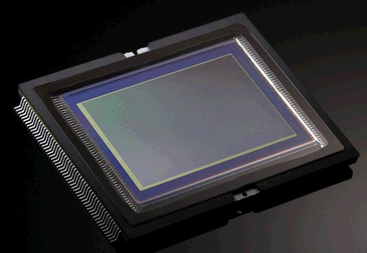
37th European Solid-State Circuits Conference (ESSCIRC) held in Helsinki, Finland, on Sept 12 - 16, 2011 had a full session on image sensors. The papers are available on-line on University of Bologna, Italy site:

A 100m-Range 10-Frame/s 340x96-Pixel Time-of-Flight Depth Sensor in 0.18um CMOS
Cristiano Niclass, Mineki Soga, Hiroyuki Matsubara, Satoru Kato
Toyota Central R&D Labs, Inc., Japan

CMOS 3D Image Sensor Based on Pulse Modulated Time-of-Flight Principle and Intrinsic Lateral Drift-Field Photodiode Pixels
Andreas Spickermann(1), Daniel Durini(1), Andreas Süss(1), Wiebke Ulfig(1), Werner Brockherde(1), Bedrich J. Hosticka(1), Stefan Schwope(2), Anton Grabmaier(1)
(1)Fraunhofer IMS, Germany; (2) TriDiCam GmbH, Germany

A CMOS Imager with Digital Phase Readout for Fluorescence Lifetime Imaging
Jian Guo, Sameer Sonkusale
Tufts University, United States

A 128-Channel, 9ps Column-Parallel Two-Stage TDC Based on Time Difference Amplification for Time-Resolved Imaging
Shingo Mandai, Edoardo Charbon
TU Delft, Netherlands

The simultaneous 41st European Solid-State Device Research Conference (ESSDERC) also had an image sensor session:

X-Ray Radiation Effect on CMOS Imagers with In-Pixel Buried-Channel Source Follower
Yue Chen(a), Jiaming Tan(a), Xinyang Wang(b), Adri J. Mierop(c), and Albert J.P. Theuwissen(a),(d)
(a) Electronic Instrumentation Lab., Delft University of Technology, Delft, the Netherlands
(b) CMOSIS nv, Antwerpen, Belgium
(c) Teledyne DALSA B.V., Eindhoven, the Netherlands
(d) Harvest Imaging, Bree, Belgium

Low-Noise Single Photon Avalanche Diodes in 0.15 um CMOS Technology
Lucio Pancheri, David Stoppa
Fondazione Bruno Kessler

Characterization of Large-Scale Non-Uniformities in a 20k TDC/SPAD Array Integrated in a 130nm CMOS Process
C. Veerappan , J. Richardson†, R. Walker‡, D.U. Li‡, M.W. Fishburn , D. Stoppa§, F. Borghetti§, Y. Maruyama , M. Gersbach¶, R. K. Henderson‡, C. Bruschini¶ and E. Charbon
Delft University of Technology, Mekelweg 4, 2628 CD Delft, Netherlands
†Dialog Semiconductor, Edinburgh, Scotland
‡University of Edinburgh, The King’s Buildings, EH9 3JL Edinburgh , Scotland
§Fondazione Bruno Kessler, via Sommarive 18, 38123 Povo, Trento, Italy
¶Ecole Polytechnique Federale de Lausanne (EPFL), 1015 Lausanne, Switzerland

Wednesday, October 12, 2011

DALSA Falcon2 Cameras Feature Fast CMOS Sensors

Market Wire: Teledyne-DALSA announced Falcon2 high resolution and high speed camera series. The new Falcon2 series includes the 4, 8, and 12M models, all based on global shutter 6um pixel:
  • Falcon2 4M delivers 4 MP at 168 fps,
  • Falcon2 8M delivers 8 MP at 90 fps
  • Falcon2 12M, delivering 12 MP at 58 fps
A Youtube video shows the sensor's features in a marketing manner:

More about Caeleste 4T Pixel with 0.5e Noise

Caeleste monthly newsletter that I was kindly offered to subscribe to has a more detailed description of its 4T pixel with 0.5e- noise:

"After reduction of kTC, EMI and thermal noise, the fundamental limit in noise in CMOS 4T pixel is the 1/f noise contribution of the source follower. It is generally accepted that the 1/f noise and RTS noise in MOSFETs is adequately explained and modeled by the McWorther theory. Charge carriers in the MOSFET’s inversion layer are captured and released, by interface states or oxide traps, acting as spurious energy levels inside the band gap. Traps that have energies close to the Fermi level of the MOSFET channel have an equilibrium occupancy probability that obeys the Fermi-Dirac statistics. For a given trap energy level, one may have a huge spread of emission and capture time constants.

In literature it is observed that this time correlation between samples can be broken by periodically pulsing the MOSFET to accumulation between samples. When returning to inversion, the long term “memory” of the trap has disappeared. The MOSFET’s noise spectrum becomes white, the signature of “uncorrelation”. Caeleste patented pixel includes a simple, compact charge trans-impedance amplifier (CTIA). The feedback capacitance is the gate-drain overlap of the driver MOSFET, and in the order of 0.1fF, resulting in an effective CVF between 1000 and 1100 μV/electron. The uncorrelation between samples allows the column electronics to reduce the (1/f) noise by Oversampling.
"

Tuesday, October 11, 2011

BBC on e2v Gaia Project

BBC runs an article on e2v supplying 106-CCD focal plane for the European Space Observatory Gaia, due for launch in June 2013. Gaia will be sent to an observing location 1.5 million km from Earth, from where it will slowly spin and scan the sky, transferring the data back at 5Mbps speed.

Although 106 CCDs were needed for the final mission, the associated development and test program meant far more CCDs were actually delivered to satellite manufacturer Astrium, which is assembling Gaia in its facilities in Toulouse, France. e2v has worked solidly for more than five years to produce all Gaia's CCDs.

"The total number of flight models and flight spares was actually 130, which is really a significant number when you think that for most of our space programmes we're talking five or six flight devices, maybe 10," explained e2v principal project manager, Roy Steward. "And then of course there were engineering and other models along the way - 44 of those. So, 174 CCDs in total."

The light-sensitive area on each CCD detector measures 45.0mm by 59.0mm, encompassing 1,966 pixels by 4,500 pixels. The slim devices are arranged in rows across a support structure made of silicon carbide, a very light and very stiff material that will not bend or warp when it experiences the temperature extremes of space. Overall, the array covers just under half a square meter and has about 1 billion pixels.

e2v's Gaia project, valued all up at about 20 million euros, has been more than just an interesting challenge. The investments allowed the Chelmsford site produce all the CCDs - buy a new cleanroom space and test equipment - meaning that it is now in a good position to compete for more space business. "Gaia forced the pace and pushed us ahead of the curve," says e2v marketing and applications manager, Jon Kemp.

Axcelis Optima HDx Selected for CMOS Image Sensor Manufacturing

PR Newswire: Axcelis announced that it has received an order for its Optima HDx high current implanter from one of the world's largest device manufacturers. The first system shipped in September and will be used to enable production of leading edge CMOS image sensors.

The implanters of this sort are used for very low-energy implants like source-drain ones, PD pinning layer or backside passivation implant. According to Axcelis white paper the energy can go down to 7KeV.

Monday, October 10, 2011

Omnivision, Broadcom and Freescale Collaborate on Automotive 360deg Camera

PR Newswire: Broadcom, Freescale Semiconductor, and OmniVision announced a jointly developed 360-degree surround view parking assistance system – the world's first Ethernet-based parking assistance solution.

  • Omnivision supplied the OV10630's 720p color HDR SoC with fully processed YUV output format.
  • Freescale brought to the plate its Qorivva MPC5604E 32-bit microcontroller with MJPEG encoding engine
  • Broadcom contributed the newly announced BCM89810 100Mbps Ethernet PHY.

"Despite the recession and delayed model cycles, reports are projecting up to 90 million parking and driver assist systems will be deployed by 2018," said Kevin Mak, automotive industry analyst for Strategy Analytics.

Imec Designed EUV Sensor for ASML

Imec announces that it has successfully qualified a chipset consisting of custom high-quality EUV sensor dies. These are now being integrated in ASML’s NXE:3100 EUV lithography tools in the field, improving the tools’ overlay and critical dimension (CD) tool performance.

The sensors were processed according to ASML’s custom designs and specifications, with focus on superior lifetime and sensitivity to direct and high EUV irradiation doses. Two of the sensors are designed to calibrate, align, and focus tool’s lens systems. They have been integrated in functional sensor modules, and are being integrated in the NXE:3100 machines in the field. A third sensor is designed to monitor the NXE:3300’s EUV dose. The next milestone in progress is to build and qualify the different sensors for the NXE:3300 by the end of 2011.

Wafer with EUV sensor dies, produced on imec's 200mm CMORE line.
Click to enlarge.

PMD CIF ToF Prototype, CamCube 3.0 demo

As mentioned in Samsung ToF sensor comments, PMD Youtube video demos its CIF-rosolution ToF camera prototype:


Another recent PMD video shows CamCube 3.0 product in action:

Kodak Bankruptcy Rumors

A week ago Bloomberg published that Kodak is weighing its options including a bankruptcy filing because of concerns raised by possible buyers of its patent portfolio, according to the three Bloomberg sources with direct knowledge of the process. Some potential bidders for the patents are wary of proceeding because a purchase may amount to a so-called fraudulent transfer if Kodak is insolvent.

A number of suitors, such as Google, have signed confidentiality agreements to examine the assets, said Bloomberg sources. If a sale was judged fraudulent, creditors may sue for more money, said one of the sources. A bankruptcy filing may help clear the way for a patent sale, said the people. The sale could fetch about $3 billion, MDB Capital Group estimates.

Kodak confirmed that it hired Jones Day to advise it on considering options and said it doesn’t plan to seek bankruptcy protection. Kodak also has discussed its options with law firm Kirkland & Ellis LLP, Bloomberg sources said.

Saturday, October 08, 2011

What Does it Take to Build an Image Sensor Company: CMOSIS Story

Imaging and Machine Vision Europe published article on CMOSIS history "Superb in CMOS". Here are the milestones:

  • Cmosis was created in November 2007 by five former employees of FillFactory, which had been sold to Cypress. The funding came from the founders, with assistance from a VC fund, totaling €1m of seed money, which is said to cover the first 18 months of development.
  • In the first year, Cmosis set itself two goals: firstly, to check that the market still had need of the specific branch of CMOS technology in which they were all experts. Secondly, the team needed to develop its new IP, which had to be tested in hardware operation, and subsequently patented, while not infringing any third party’s (including FillFactory’s) IP.
  • At the end of that first year, Cmosis had filed two patents: 8T fully pipelined global shutter pixel and fast column-level ADC
  • During that first year, Cmosis also worked on its first custom design contract. This had the benefit of generating revenue at an earlier stage than perhaps Cmosis was expecting.
  • An intermediate round in 2008, with the same investors, brought another €1m.
  • With IP developed and a custom design contract in hand, the team was able to pursue another round of financing in August 2009, this time for a further €3m, with the help of a bank and some government supported investment funds. The money were used to move to larger offices, install a cleanroom, buy a wafer probing station. The company also invested in its infrastructure and expanded its team.
  • First standard image sensor products for the machine vision market – the 2.2MP/340fps CMV 2000 and 4.2MP/180fps 4000, launched at the Stuttgart Vision show in Nov 2009.
  • Leading names in the machine vision industry have adopted the sensors for their camera ranges, including Basler, Point Grey Research, IO Industries and Adimec.
  • Sept. 2011, Cmosis has 35 employees based at its headquarters in Antwerp, Belgium.
  • Future plans include the launch of a new product at the Vision show later this year, aimed at the lower end of the market.
Funding in 2009 allowed the company to invest in
cleanroom facilities and a wafer prober for wafer testing

Friday, October 07, 2011

poLight AF Speed

EETimes-Europe published poLight article comparing its TLens with VCM-driven AF lens in terms of speed and accuracy:


poLight shows that its AF speed is pretty much limited by the sensor's framerate:

Computational Imaging Review

Columbia University published Oliver Cossairt's PhD thesis "Tradeoffs and Limits in Computational Imaging" reviewing broad range of modern technologies, such as EDoF, plenoptic cameras, gigapixel cameras, etc. Some conclusions from the thesis:

Figure 1.7: EDOF cameras sacrifice best case performance for average case performance. The performance is measured as the MTF of the camera system as a function of depth.

Figure 2.1: Simulated image performance for three EDOF cameras. An IEEE resolution chart is placed at different depths. The aperture size A and defocus slope in light field space s0 are chosen so that the maximum defocus blur diameter is 100 pixels. The center PSF is used for deblurring, producing the images shown in (b). Close-ups in (c) show that the sharpest image is produced by wavefront coding at the center depth (s0A = 0). However, wavefront coding produces significant deblurring artifacts for defocus values as small as s0A = 33 pixels, while diffusion coding produces near identical results for the entire depth range.

Spectral Focal Sweep EDoF technology is proposed, similar to DxO one, but said to perform better:

Figure 1.9: Performance vs. Complexity for the Spectral Focal Sweep camera (see Chapter 3). A conventional camera achieves higher performance than the Spectral Focal Sweep camera, but at the cost of a significant increase in complexity.


Figure 1.8: Resolution scales rapidly with camera size for ideal diffraction limited lenses. However, in practice, resolution reaches a plateau due to geometric aberrations. The Gigapixel Computational Camera introduced in Chapter 3 breaks the aberration limit so that resolution continues to increase with camera size, despite the presence of geometric aberrations.

Figure 4.6: For conventional lens designs, the F/# typically scales with the cube root of the focal length in millimeters.

Figure 4.11: Scaling laws for computational imaging systems with spherical aberrations. The Rana, which was analytically derived, shows an improvement upon the aberration limited curve Rgeom, without requiring F/# to increase with M. Performance is further improved when natural image priors are taken into account, as the Rprior curve shows. The Rprior curve improves upon the conventional lens design curve Rconv, also without requiring F/# to increase with M.

Thursday, October 06, 2011

Samsung Presents 1/3-inch QVGA ToF Sensor

Samsung published Youtube video presenting the new 1/3-inch QVGA ToF Sensor - the S5K32D:


Samsung S5K32D QVGA 1/3" TOF Sensor is said to have high resolution and high speed for Z-axis User Interface. The text abstract also says that it's:
  1. World's first QVGA resolution TOF Sensor
  2. Supporting high speed frame rate
  3. One Chip solution for depth image

Update 2012/02/20: The updated Samsung web site lists 3D ToF part as S5K32A. The pixel uses BSI technology and is of 14um size.

2nd Workshop on CMOS Image Sensors for High Performance Applications

A program has been announced for the 2nd workshop "CMOS Image Sensors for High Performance Applications", co-organized by CNES, Astrium and Thales Alenia Space, to be held on December 6th-7th, 2011 in Toulouse (France). Along these two days, 27 talks about high performances CMOS Image Sensors will be presented by 22 teams from industries, institutes, labs and agencies:

  1. Characterization Results of Teledyne-DALSA High Bandwidth Matrix and Linear CMOS Devices and Roadmap for Radiation Hard and High Resolution Area Devices
    COCHRANE David (TELEDYNE-DALSA)
  2. High QE, Thinned Backside-Illuminated, 3e- RoN, Fast 700fps, 1760x1760 Pixels Wave-Front Sensor Imager with Highly Parallel Readout
    DOWNING Mark (ESO)
  3. Fast-Response, Low-Noise, Multiple Shutter, Non-Destructive Readout Line Sensor for Spectroscopy Applications Based on Lateral-Drift-Field Photodiode Principle
    DURINI Daniel (Fraunhofer Institute)
  4. L²CMOS Image Sensor for Low Light Vision
    FEREYRE Pierre (e2v)
  5. First Results from Single Photon Avalanche Diodes Manufactured in a 0.18 μm CMOS Image Sensor Technology
    COATH Rebecca (STFC)
  6. ESA supported developments in CMOS Imaging Sensors
    NELMS Nick (ESA-ESTEC )
  7. Survey of CMOS devices developped by Astrium-ISAE for ESA LEO and GEO missions
    BREART DE BOISANGER Michel (EADS Astrium)
  8. Survey of CMOS devices developped by Astrium for Ocean Colour Imaging from GEO
    BREART DE BOISANGER Michel (EADS Astrium)
  9. CMOS image sensor for lunar mission
    WANG Weng Lyang ‘Bill’ (CMOS Sensor Inc.)
  10. High-Speed BSI CMOS Image Sensor for Space Applications with 1.1Me- Full Well Capacity and 28e- rms Read Noise
    VU Paul (BAE Systems Imaging Solutions)
  11. CNES roadmap for CMOS image sensors in Space applications
    MATERNE Alex (CNES)
  12. Characterization of a Digital TDI CMOS demonstrator
    LEPAGE Gérald (CMOSIS)
  13. Monolithic, 120 mm CMOS sensor for Multi-mode RSI application
    LO Shih-Hung ‘Redman’ (NSPO)
  14. Developments of back side illuminated CMOS APS for EUV Solar Observations
    BENMOUSSA Ali (STCE Royal Observatory of Belgium)
  15. Digital Focal Plane arrays for Cooled Infrared Detectors
    DECAENS Gilbert (SOFRADIR)
  16. IR Sensors for space applications at Selex Galileo
    WELLER Harald (SELEX GALILEO)
  17. Innovative ROIC for very low flux sensors
    SANSON Eric (SOFRADIR)
  18. Specifications of an Analog-to-Digital Converter For uncooled infrared readout circuits.
    ROBERT Patrick (ULIS)
  19. CTIA circuit for low light level imaging with InGaAs detector.Demonstration with a 15μm pitch VGA format
    GUELLEC Fabrice (CEA-LETI)
  20. A 2 photon noise 2 KHz frame rate, with in-pixel CDS, IR sensor for Adaptative Optic Applications
    SALVETTI Frédéric (SOFRADIR)
  21. Optimisation of performance of Backthinned CMOS devices
    JERRAM Paul (e2v)
  22. Results of the second generation hybrid backside illuminated imagers and an introduction to other high-end imager developments at imec
    MINOGLOU Kiki (IMEC)
  23. Outstanding properties of Espros Photonic CMOS process for high performance imaging
    POPP Martin (Espros Photonics AG)
  24. A Common Gate Pinned Photodiode Pixel
    DE WIT Yannick (ON Semiconductor)
  25. Reduction of pixel 1/F noise by inversion/accumulation cycling
    DUPONT Benoît (CAELESTE)
  26. Radiation Effects on CMOS Image Sensors
    VIRMONTOIS Cedric (ISAE)
  27. Performance of deep submicron CMOS image sensors after radiation
    BERNARD Marie (CNES)

The workshop is free of charge. One can register here: http://cnes.cborg.net/cct/bipublicgb.html

Thanks to AT for sending me the program!

Yole Predicts 75um Thin CIS Wafers in 2014

Yole Développement's report "Thin Wafer Market & Applications" predicts that thinned wafers will reach 50% of all wafer shipments in 2016, up from 27% today. "Motivations for thin wafers are: high interconnect density (such as aggressive TSV pitch & diameters), better power dissipation and higher electrical performance and reduced package size."

Here is how image sensor wafer thickness looks in comparison with others:

Wednesday, October 05, 2011

Small Pixels and Machine Vision

Adimec blog published a post on small pixel potential in machine vision applications: "Can small pixel CMOS image sensors be useful in Machine Vision?"

The conclusion is: "There is a trend towards using smaller pixels for machine vision applications leveraging technology developed for the high volume consumer camera applications. However the requirements for machine vision are very different and it will take some time before the image sensor pixels have high enough performance to make it into the machine vision cameras."

Tuesday, October 04, 2011

Oppenheimer Research Speculates that Omnivision is Inside iPhone 4S

Oppenheimer Research note states that Omivision is likely inside the newly announced iPhone 4S. The #1 reason is:

"Apple in its iPhone release presentation mentioned that the image sensor is a 8MP sensor with the description 3264 pixels X 2448 pixels resolution or 7.99MP. It is spot on with OVTI's 8830 spec, whereas Sony's 8MP spec is 3288 X 2472 or 8.12MP."

Update: More analyst's speculations:

Barrons: R.W. Baird’s Tristan Gerra writes that his “field research” suggests Omnivision has lost some share to Sony in the 4S, citing anecdotal evidence that the Sony part matches the phone’s specs.

Various websites report these Sony Ericsson smartphones feature a Sony image sensor of the exact size as for the iPhone 4S (3264×2448),” he writes, adding, “Additionally, image sensor makers typically customize their sensors specifically for Apple without necessarily releasing the specs.

But JP Morgan’s Paul Coster comes to the stock’s defense, noting that Apple describes an a larger “active array size” to the iPhone’s sensor. That, he suggests, implies the phone uses OmniVision’s “OVT8830 CIS” chip. “The iPhone 4s sensor active array was announced to be 3264 by 2448, which is an exact match for the Omnivision OVT8830 first-generation BSI image sensor,” writes Coster, “We note that Sony’s IMX105PQ 8MPx chip has a 3288 by 2472 array.

Motley Fool writes, again relying mostly on the sensor format: "I think I've built a pretty compelling case here for the OV8830. Dual-sourcing a component this important just doesn't fit Apple's modus operandi."

Brookman Technology Presentation

Youtube video from few months ago shows Brookman Technology presentation, including a short company story, a talk about 1.3MP/2000fps fast sensor with global shutter and 5.6um pixels, and sub-electron noise 16b DR sensor with 7.5um pixels demoed at 0.03 lux/F1.4/10fps:

Chipworks Reverse Engineers CMOSIS Sensor

Chipworks published CMOSIS fast 4MP/180fps CMV4000 reverse engineering. The sensor features fully pipelined global shutter. The report covers the imager process.


It's Official Now: Nobukazu Teranishi Received 2011 PSA Progress Medal

For some odd reason, there was no official news report on the award. Now there is - Photographic Society of America Fall Newsletter has an article on Nobukazu Teranishi receiving 2011 PSA Progress Medal Nobukazu Teranishi at the Final Banquet of the 73rd Annual Conference of Photography held in Colorado Springs, Colorado.

Nobukazu Teranishiis the General Manager in the Image Sensor Business Unit in Japan. He has been an influential technical leader in the development of both CCDs and CMOS sensors for 31 years, and accomplished the following three key technologies:

  1. the pinned photodiode for no image lag, low noise and low dark current
  2. technologies to prevent high light deterations
  3. mega –pixel technologies for HDTV cameras and digital still cameras.

Almost all CCD’s and CMOS sensors use pinned photodiodes now and 200 million CCD’s and one billion CMOS sensors were produced in 2008.

Monday, October 03, 2011

Invisage Reveals Few More Bits of its Technology

Invisage patent applications US20110228144 and US20110226934 have been published. The US20110228144 is titled "DARK CURRENT REDUCTION IN IMAGE SENSORS VIA DYNAMIC ELECTRICAL BIASING" and shows how Invisage plans to reduce sense node diffusion dark current in what looks like a typical 3T pixel:


Invisage approach is quite simple - precharge the sense node to zero voltage so that in the dark the sense node voltage is always zero. Here is the timing diagram and the description (I used slightly wrong pixel figure because it has better labeling. The photocurrent direction is wrong):


"During a first period labeled “True reset,” the diode, or charge store, is reset to a known reference point, by setting the reset electrode to high voltage (turning on the reset transistor M1). In embodiments, during the reset phase, the electrode vfilm (i.e., the biasing electrode) is set to a bias voltage that is higher than diode voltage, for example 3V (normal range from −5V to 5V). The pixel electrode diode is driven to be a lower voltage, for example 0V (normal range from 0V to 5V). This is achieved by setting VLEVEL to a low voltage.

During a second period labeled “Integration,” the electrode vfilm remains at the same voltage, for example 3V. Light induced photocurrent in the floating photodetector will drive the diode voltage higher. The photocurrent serves as a current source in this configuration. The use of a low voltage on the pixel electrode significantly suppresses the dark current of the pixel circuitry under a dark condition. VLEVEL is pulled back to high voltage such as 3V, to minimize leakage path of transistor M1, and to prepare for readout phase.

During a third period labeled “Read signal,” the electrode vfilm is brought to a higher level, such as 5V (normal range −5V to 5V). This will boost up the diode voltage to make sure the low voltage at diode node can be read out through the readout circuit, and thus maintain dynamic range for the readout path. Alternatively, a low VT readout transistor M2 (for example, threshold of 0V, with range of −1V to 1V) can be used to read out the low voltage, in which case the pulsing on common electrode is not necessary.

During a fourth period labeled “CDS reset,” the reset electrode goes high again, setting the diode voltage to the same known level. This is achieved by pulling VLEVEL to the same low voltage as in ‘true reset’ phase.

During a fifth period labeled “Read reset,” VLEVEL is pulled back high to allow M2 functions as a readout transistor. This phase is used to readout the reset level.
"

The idea is quite nice but what about Reset transistor M1 charge ingection variations due to pixel-to-pixel mismatch? One can not allow sense node to go negative, so the average sense node voltage should be high enough to keep worst case pixel in positive domain. This can easily be 50mV or so for the average pixel. At this voltage the dark current would be lower, but not zero.