After more than half year with no image sensor news, May 2010 Hynix newsletter announces Hi-704, new 1/10-inch VGA sensor packaged in Tessera ShellUT CSP. The sensor uses 2.25um pixels and features single 2.8V supply and 30fps speed at its full VGA resolution. Samples were available in March 2010, mass production has started in May 2010.
The new sensor appears to be a single-supply and a different package version of another VGA sensor announced in October 2010.
So far, Hynix portfolio appears to be skewed towards low-end sensors. With going prices of 35-40 cents per VGA die, I wonder where Hynix is aiming? Is competing with Galaxycore, SETi and low-end Omnivision sensors where Hynix sees its future?
Monday, May 31, 2010
Friday, May 28, 2010
Omnivision Q4/FY2010 Earnings Call
Seeking Alpha published Omnivision Q4/FY2010 Earnings Call. Talking about BSI progress Omnivision says:
Shaw Hong, CEO:
"The BSI shipment ramp provide an improvement in our product mix during the fourth quarter [last quarter, that is], with a concentration of OmniBSI primarily in our higher-resolution devices. In particular, we are pleased with the continue market share gain of our 5- and 8-megapixel devices in the mobile phone and DSC markets in which are now in full mass production with several major customers."
Omnivision was quite cautious commenting on its BSI technology lead over competitors in the following question:
Betsy Van Hees - Wedbush Securities:
"So when you look into competition though, how far does that [BSI] lead stay ahead? Is anyone catching you? Or are you just going to continue to dominate the field in this area?"
Bruce Weyer, VP WW Marketing:
"So we hear of competitors starting to potentially sample products, but sampling products and meeting the performance goals of our customers could very well be different things. It does take a while to perfect these types of technologies. So I'm not in a position to fully state where they're at in their development process, but based on our sampling window to strong leadership position, we think we're in a pretty good shape."
Ray Cisneros, VP WW Sales:
"And just another comment about that. It's going from sampling to mass production in tens of millions of units per quarter, that's the big learning curve that everybody's got to go through. And as Bruce mentioned, it's difficult to understand where our competition is in that curve. But suffice it to say from our side, it's a learning curve that's not easy and it's not overnight."
On the WLC becoming a primary handset camera:
Yair Reiner - Oppenheimer & Co.:
"...in terms of the wafer-level camera, I know you've been trying to get that into design as a primary camera, kind of a lower-end feature phone. How is that coming, and when do you think there's a chance to start shipping that in volume?"
Ray Cisneros:
"Well, we're shipping wafer-level module, a product today. ...its primary application is secondary video cameras for handsets. The nirvana or the end goal of many of these products is to be the primary camera for handsets as well as for other products. But it's going to be a learning curve for both sides, the supplier side, ourselves as well as the our customers' side, to understand where exactly that fits and when does it fit in. On top of that, there are some technological hurdles that most people are working on which are optical advancements. So it's in progress. I'd imagine it's going to take a few quarters before that is fully captured in primary applications."
On the product and market split:
Ray Cisneros:
"...unit sales of sensors that were VGA below were approximately 60% in the fourth quarter. Our wafer-level module shipments were approximately equivalent compared to the prior quarter.
...Unit sales of 1.3-megapixel sensors increased to approximately 12% of total shipments.
...unit sales of sensors 2-megapixel and higher increased... to approximately 27% of total shipments.
In terms of product markets, our mobile phone sales represented approximately 55% of our revenues in the fourth quarter. Notebook and PC sales were approximately 30% of revenues in the quarter. Sales of our other emerging market products accounted for approximately 15%."
Pixelplus Reports Q1 2010 Results
PR-Newswire: Pixelplus revenue for the Q1 2010 was US$3.6M, compared to US$5.3M in Q4 2009, and US$3.1M in Q1 2009. Net income in Q1 2010 was US$0.3M, compared to a net income of US$1.8M in Q4 2009, and a net loss of US$1.0M in Q1 2009.
The company sold roughly 1.6 million image sensors in Q1 2010, which represented a decrease of about 2.4 million from its sale of around 4.0 million units in Q4 2009. Separately, the Company furnished approximately 0.06 million image sensors arising from its supply of services to a leading Japanese module maker in Q1 2010, which represented a decrease of about 0.04 million units from its supply of around 0.1 million units in the Q4 2009.
Gross margin for the first quarter of fiscal 2010 was 40.5%, compared to 44.5% in the fourth quarter of fiscal 2009. The company's high gross margin was mainly due to its sale of high margin-driven products and service revenues.
Omnivision Reports Quarterly and Yearly Results
PR-Newswire: Omnivision reported financial results for the fiscal fourth quarter and fiscal year ended April 30, 2010. Revenues for the fourth quarter of fiscal 2010 were $157.2M, as compared to $156.9M in the third quarter of fiscal 2010, and $89.1M in the fourth quarter of fiscal 2009. GAAP net income was $3.5M, as compared to net income of $5.0M in the third quarter of fiscal 2010, and a net loss of $20.1M in the fourth quarter of fiscal 2009.
Revenues for the fiscal year ended April 30, 2010 were $603.0M, as compared to $507.3M in fiscal 2009. The Company ended the period with cash, cash equivalents and short-term investments totaling $333.6M.
Gross margin for the fourth quarter of fiscal 2010 was 24.9% as compared to 24.6% for the third quarter of fiscal 2010 and 17.0% for the fourth quarter of fiscal 2009. The sequential increase in fourth quarter gross margin reflected a reduction in the revenues recorded from the sale of previously written-down inventory net of additional allowances for excess and obsolete inventories.
The company expects fiscal first quarter 2011 revenues will be in the range of $190M to $210M.
Thursday, May 27, 2010
Aptina WDR Sensor Features in Bar Code Reader
Business Wire: Code Corporation announces that its new CR8000 bar code reader features Aptina's MT9M033 WDR image sensor. Code began collaborating with Aptina on its new product during the summer of 2009. “We had very strict product requirements, and the Aptina MT9M033 was the clear choice in meeting the needs of our product roadmap for the next five to seven years,” said Garrett Russell, VP of Marketing for Code Corporation - It's nice to see such a loyal customer.
BSI Manufacturing and Equipment
ElectroIQ published Yole Développement article on BSI and WLC as the next generation drivers of image sensor technology. A quote below describes BSI porcess and manufacturing equipment:
"The BSI process flow starts with making the photo diodes. Then the device wafer is bonded at low temperature to a silicon or glass carrier, using either adhesive polymers or molecular oxide-to-oxide bonding. US-based 3D-IC company Ziptronix offers one low-temperature bonding solution, which presses together ultraflat wafers, well prepared through specific surface preparation treatments. Next, the 1mm thick photo diode wafer is thinned down to 40-50μm with Disco or Accretech grinding tools, then thinned further with CMP, and finally etched down to an etch-stop layer at 5μm. This radical wafer thinning typically requires precise control of wet etching after initial grinding and CMP. One option, used by Sony and others, is to use SOI wafers from Soitec, using the buried oxide layer as an inner etch stop layer at the oxide interface -- though the high cost of SOI wafers may limit the process to high-end imaging applications only. Others, including OmniVision, working with TSMC and Xintec, claim to have developed a lower-cost alternative process using bulk silicon wafers with graded implant layers. The trick is to find a highly selective etch chemistry that will stop precisely at the required 5μm thin silicon interface, just before reaching the photodiode structures.
Also critical is the annealing process, since this 5μm thin silicon film needs to include a very narrow implant gradient, to prevent recombination in the epi silicon and to push the photons down to the photo diodes. Since typical annealing ovens can only be controlled to about 30μm layer precision, the finer implant gradients require annealing with a nano-second, local heating laser process. The French equipment company Excico supplies a tool that uses a UV excimer type of laser source with a large spot for tight precision with better image quality and higher throughput."
The article also overviews the wafer level camera AF approaches:
"Companies are also working on integrating autofocus functions at the wafer level. A number of players, including SEMCO, are working on electro active polymers, whose thickness can be controlled and driven electrically by applying a defined voltage. Others like Siimpel (recently acquired by Tessera) have a MEMS- based solution, using a spring-like silicon structure.
But the front-runner currently appears to be a potentially breakthrough technology using liquid crystal polymers. The startup LensVector plans to start production this year of a four-layer stack of 8-in. glass wafers, encapsulating liquid crystal polymers that change shape when voltage is applied to the driving electrodes -- all in less than 500μm total thickness. This technology has the potential to significantly bring down the size and cost of camera modules in the future."
Wednesday, May 26, 2010
NHK Continues to Improve Organic Image Sensor
Tech-On: NHK Science & Technology Research Laboratories (STRL) is going to showcase a full-color organic image sensor, which is a CMOS image sensor made by stacking an organic semiconductor material as a photosensitive layer on a transparent TFT array. The sensor has a resolution of 128 x 96 pixels for each of the RGB colors. NHK installed the sensor in a camcorder so that it can shoot color video. The TFT array was developed based on zinc oxide (ZnO) in collaboration with the Kochi University of Technology.
The company plans to develop organic image sensors in 10 years for HD camcorders and in 20 years for super high vision camcorders.
The company plans to develop organic image sensors in 10 years for HD camcorders and in 20 years for super high vision camcorders.
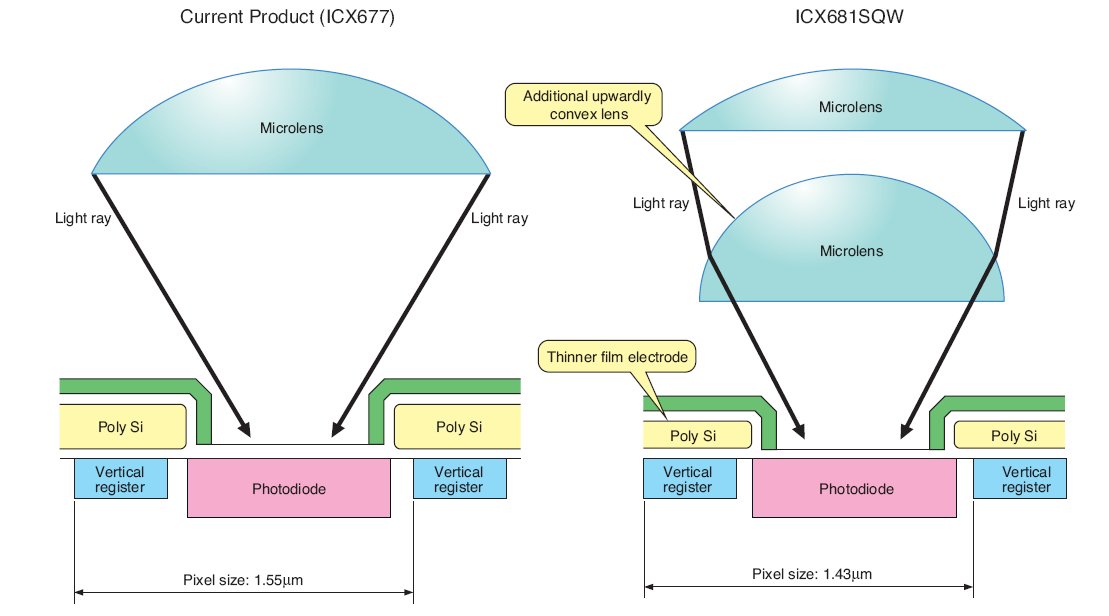
Sony Shrinks CCD Pixel to 1.43um
Sony announces industry smallest pixel size CCD in the recently published Cx_News vol. 60. 14.2MP ICX681SQW features 1.43um pixel, on par with the modern CMOS sensors in production. To improve the light collection efficiency Sony uses dual microlens:

Other notable features are reduced by 12% power consumption and 1/4 resolution mode for high sensitivity and high speed image capture (5.4fps at 3.55MP resolution).
Another Cx-News article digests Tomoyuki Suzuki, Sony SVP keynote at ISSCC 2010 on Image Sensor Evolution and the Future of Imaging.
Other notable features are reduced by 12% power consumption and 1/4 resolution mode for high sensitivity and high speed image capture (5.4fps at 3.55MP resolution).
Another Cx-News article digests Tomoyuki Suzuki, Sony SVP keynote at ISSCC 2010 on Image Sensor Evolution and the Future of Imaging.
Mentor Graphics is Optimistic about Image Sensor Market
Mentor Graphics published its CEO Walden Rhines keynote at last year's Semicon West presenting the company view on image sensor market, among many other things. The keynote looks like an extended version of an EETimes article quoted here before. One must say that Mentor picture is quite optimistic:


Monday, May 24, 2010
inSilica Status
ISP IP vendor inSilica's web site has died. inSilica used to have one of the best ISP design teams split between Slovenia and India. Web snapshots of the site show that it was alive at the end of April.
Incidentally, Linked-In records show that a number of inSilica employees located both in Slovenia and in India have all started to work for Aptina since March 2010 (India-1, India-2, India-3, Slovenia-1, Slovenia-2, Slovenia-3). Also, one of Linked-In recommendations says that Aptina worked with Insilica "on a key new product" for more than 14 months.
It would be great if somebody can shed a light on what happened with inSilica.
Update: As said in comments, Aptina has acquired inSilica assets, including its India and Slovenia teams.
Friday, May 21, 2010
First Full-HD Camera Phones Announced in Japan
Tech-On: NTT Docomo announced Fujitsu F-06B and Sharp SH-07B camera phones, which NTT Docomo claims are the world's first mobile phones capable of shooting full HD video. Both phones rely on Renesas SH-Mobile G4 combined baseband/application processor for 1080/24fps HD video processing.
Thursday, May 20, 2010
Eric Fossum Receives NYIPLA Inventor of the Year Award
Eric Fossum received the 2010 Inventor of the Year Award from the New York Intellectual Property Law Association (NYIPLA) for his extensive portfolio of patents related to CMOS active pixel image sensors and the so-called “camera on a chip technology” that is at the heart of technologies ranging from cell phone cameras to swallawable pill cameras.
Wednesday, May 19, 2010
Sony Sensor in Microsoft Kin
Chipworks teared down Microsoft Kin Two and revealed that is uses Sony 8MP IMX046 sensor featuring a five metal 90nm process and 1.4µm pixel size.
Tuesday, May 18, 2010
Aptina Explains its BSI-FSI Strategy, Announces New Sensors
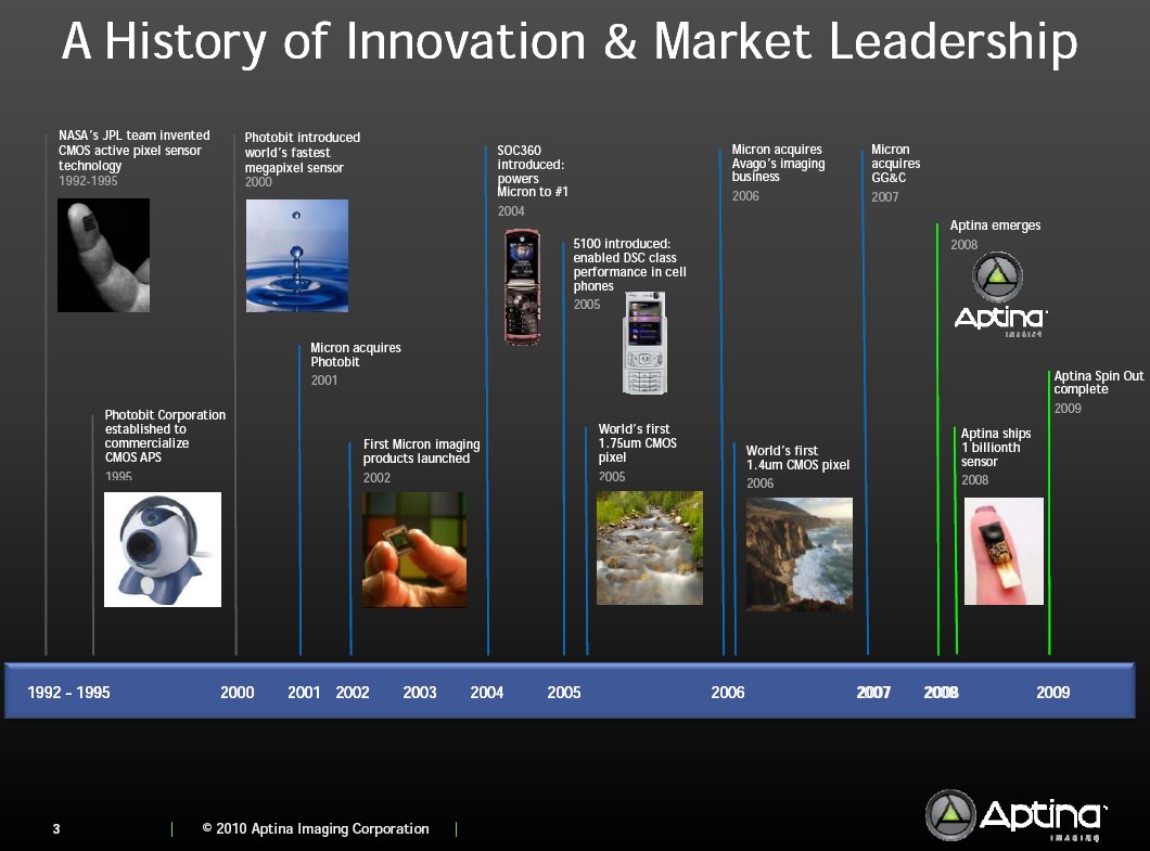
Business Wire: Aptina made few big announcements today explaining its A-Pixel technology, FSI and BSI pixel plans and also launched two new sensors. I was given a media kit accompanying these announcements. The pictures below are from this kit.
The corporate presentation says that Aptina has achieved $547M sales in 2009 and the company has about 700 employees. Aptina's historical milestones are shown on the slide below:

The most interesting part here is an acquisition of GG&C in 2007. I do not recall any official announcements about that. A quick search on Linked-In shows that GG&C developed a telescope with extended depth of field.
Market share slide is rarely seen chart based on revenue, rather than units. It shows quite different picture from the unit market shares:

Next slide shows conflicting requirements of stills photography and video, with video mostly demanding low light:

This results in Aptina FSI vs BSI approach:

Here comes the explanation of Aptina A-Pix advantages - combination of deep photodiode with lightguide results in improved light sensitivity:

Next slide says that BSI is not really necessary at 1.4um pixel node, if one has 65nm process instead. First BSI products will be announced in the second half on this year at 1.1um node:

3rd generation A-Pix features better fill factor dues to thinner metals in 65nm process:

Aptina FSI vs BSI whitepaper says about BSI problems:
"For 1.4 micron BSI pixels, QE is typically in the 50-60 percent range with crosstalk in the 15-20 percent range. The combination of BSI’s high QE and somewhat degraded crosstalk at 1.4 micron results in a net overall image quality that is comparable to FSI for 1.4 micron pixels.
Today, 1.1 micron BSI pixels are still in the early stages of development, but when they are production-ready, they would be expected to have a QE approaching 50-60 percent with crosstalk in the 10-30 percent range. These 1.1 micron BSI pixels should be outperforming 1.1 micron FSI pixels at that point due to the fabrication challenges in shrinking FSI pixels to 1.1 micron.
A tipping point for BSI will be the 1.1 micron pixel node where FSI will likely be unable to achieve the market-required performance – necessitating a transition to BSI for applications that require this smaller pixel."
Additionally, Aptina announced two new sensors based on 3rd generation 1.4um A-Pix technology: the 3MP SOC MT9T113 and the 5MP MT9P017. Both sensors have small die size suited for integration into 6.5 x 6.5 mm modules, parallel and MIPI interfaces and integrated AF VCM driver.
The 1/5-inch MT9T113 SOC features JPEG thumbnail support, Scalado SpeedTags and 720p/30fps HD video. The 1/4-inch MT9P017 has adaptive noise reduction, 2D dynamic defect correction, and supports 1080p/30fps or 720p/30fps HD video.
Update: There is Youtube video with A-Pix explanations by Gennadiy Agranov, Aptina's VP of Imaging Technology:
Update #2: EETimes published an article on the new Aptina announcements.
The corporate presentation says that Aptina has achieved $547M sales in 2009 and the company has about 700 employees. Aptina's historical milestones are shown on the slide below:
The most interesting part here is an acquisition of GG&C in 2007. I do not recall any official announcements about that. A quick search on Linked-In shows that GG&C developed a telescope with extended depth of field.
Market share slide is rarely seen chart based on revenue, rather than units. It shows quite different picture from the unit market shares:

Next slide shows conflicting requirements of stills photography and video, with video mostly demanding low light:

This results in Aptina FSI vs BSI approach:

Here comes the explanation of Aptina A-Pix advantages - combination of deep photodiode with lightguide results in improved light sensitivity:

Next slide says that BSI is not really necessary at 1.4um pixel node, if one has 65nm process instead. First BSI products will be announced in the second half on this year at 1.1um node:
3rd generation A-Pix features better fill factor dues to thinner metals in 65nm process:

Aptina FSI vs BSI whitepaper says about BSI problems:
"For 1.4 micron BSI pixels, QE is typically in the 50-60 percent range with crosstalk in the 15-20 percent range. The combination of BSI’s high QE and somewhat degraded crosstalk at 1.4 micron results in a net overall image quality that is comparable to FSI for 1.4 micron pixels.
Today, 1.1 micron BSI pixels are still in the early stages of development, but when they are production-ready, they would be expected to have a QE approaching 50-60 percent with crosstalk in the 10-30 percent range. These 1.1 micron BSI pixels should be outperforming 1.1 micron FSI pixels at that point due to the fabrication challenges in shrinking FSI pixels to 1.1 micron.
A tipping point for BSI will be the 1.1 micron pixel node where FSI will likely be unable to achieve the market-required performance – necessitating a transition to BSI for applications that require this smaller pixel."
Additionally, Aptina announced two new sensors based on 3rd generation 1.4um A-Pix technology: the 3MP SOC MT9T113 and the 5MP MT9P017. Both sensors have small die size suited for integration into 6.5 x 6.5 mm modules, parallel and MIPI interfaces and integrated AF VCM driver.
The 1/5-inch MT9T113 SOC features JPEG thumbnail support, Scalado SpeedTags and 720p/30fps HD video. The 1/4-inch MT9P017 has adaptive noise reduction, 2D dynamic defect correction, and supports 1080p/30fps or 720p/30fps HD video.
Update: There is Youtube video with A-Pix explanations by Gennadiy Agranov, Aptina's VP of Imaging Technology:
Update #2: EETimes published an article on the new Aptina announcements.
e2v CCD on the Way to Venus
RF Globalnet: On May 17, 2010, e2v CCDs are (were) due to be launched into space on board the Japan Aerospace Exploration Agency's (JAXA) Venus Climate Orbiter "Akatsuki" (formally known as PLANET-C) to study the planet Venus. e2v CCD47-20 sensors equip the Ultraviolet Imager (UVI) onboard Akatsuki. It is a frame transfer CCD, with 1024 x 1024 pixels, each 13µm square. The device is back-illuminated, with optimised processing and coatings for performance in the 280nm – 365nm wavelength range. It is housed in a hermetically sealed package, with a sapphire window also optimised for transmission in the UV range.
Monday, May 17, 2010
Duisburg CMOS Imager Workshop Review is Complete Now
Albert Theuwissen has completed his review of papers presented on CMOS Imager Workshop in Duisburg, May 4-5, 2010.
Omivision Releases 1.4um BSI 1080p Video Sensor
PR-Newswire: Omnivision introduced the OV2720, a 1/6-inch, native 1080p/30fps HD image sensor notebook, netbook, webcam and video conferencing applications. Based on 1.4um OmniBSI features sensitivity of 680-mV/lux-sec, and enables extremely thin modules with a z-height of 3.5 mm.
The OV2720 is currently sampling with multiple tier-one customers and is slated to go into mass production in June 2010.

The OV2720 is currently sampling with multiple tier-one customers and is slated to go into mass production in June 2010.

Diffusive-Coded EDoF
As Electrons and Holes blogger noticed, Columbia University team is doing a nice work on using a light diffuser to determine depth and implement a diffusive-coded EDoF (SIGGRAPH 2010 paper).
Samsung Products List, Current and Future
As Bart mentioned in comments, Samsung has a nice list of CIS products, including future products under development now. The list shows a couple of 1.1um and 1.12um pixel-based sensors.
Update: To make post shorter, only 1.1um planned products are shown below:
Update: To make post shorter, only 1.1um planned products are shown below:
| part number | Production Status | Product Type | Resolution | Pixel Size | Optical Format | Frame Rate | Package |
| S5K3L1Y | Under Development | Sensor Only | 4000 x 3000 (effective) | 1.12um | 1/3.2 | 15fps | Wafer, Die |
| S5K2N1Y | Under Development | Sensor Only | 4400x3300 | 1.10um | 1/2.33 | 15fps | Wafer, Die |
Saturday, May 15, 2010
OmniBSI-2 Promotional Video
A promotional OmniBSI-2 video appeared at Youtube:
Among many general PR statements there is an interesting performance comparison graph in the video, although QE numbers on the right look out of sync with the graph:

Update: The above graphs present comparison for the same pixel size, as said in video.
Among many general PR statements there is an interesting performance comparison graph in the video, although QE numbers on the right look out of sync with the graph:

Update: The above graphs present comparison for the same pixel size, as said in video.
Aphesa Tutorial on Si Sensors Spectral Response
Belgian consulting company Aphesa published a nice tutorial on silicon-based image sensor spectral response.
Friday, May 14, 2010
Samsung Mysterious DSLR Sensor with Pseudo-Multi Sample Readout
K-Rumors published a mysterious story about new Samsung sensor for DSLR, the S5K1N2. The 14.2MP APS-C imager features Pseudo-Multi Sample (P-MS) circuit coupled with column-parallel dual slope ADC. The readout is said to support Multi-Sample mode and deliver 10.7fps at full resolution through its 8 outputs. The video mode is full HD 1080p/60fps. The sensor is based on 5.1um pixels.
Thanks to A. for sending me the link!
Thanks to A. for sending me the link!
Delft Sensor and Imaging Symposium Presentations On-Line
Delft University "Sensors and Imaging: A VLSI Design Perspective" Symposium materials are available on-line. The Symposium was held on Dec. 7, 2009.
Unfortunately, the most interesting presentation "State-of-the-art and future perspectives of Back-Side Illumination" by Albert Theuwissen is not not available for download.
Another interesting presentation from Fondazione Bruno Kessler of Trento, Italy talks about 3D camera principles:
David Stoppa, Fondazione Bruno Kessler FBK-IRST, Italy
Pixel Architectures for Time-Resolved Imaging Applications
There are 4 TOF pixel architecture covered. The presentation does not talk about any of the commercially available cameras, like PMD, Canesta, MESA, Optrima.
Just a few days ago, on May 5, Fondazione Bruno Kessler announced that it's demoing its first 3D camera prototype. While the announcement does not give any technical details, one can guess that the camera is based on the sensor presented at ISSCC2010:
David Stoppa, Nicola Massari, Lucio Pancheri, Mattia Malfatti, Matteo Perenzoni, and Lorenzo Gonzo, "An 80x60 Range Image Sensor based on 10um 50MHz Lock-In Pixels in 0.18um CMOS", ISSCC 2010
Another interesting presentation from the Delft Symposium is Orly Yadid-Pecht one, talking about HDR schemes and active pixel reset ideas:
Orly Yadid-Pecht, University of Calgary, Canada
Advances in a CMOS Image Sensor based miniature fluorsence Detection System for Biosensing Applications
Wednesday, May 12, 2010
Albert Theuvissen Continues CMOS Imager Workshop Review
Albert Theuwissen reviews Day 2 of CMOS Imager Workshop in Duisburg, Germany. This part includes Fairchild sCMOS sensor, Alexima and CMOSIS presentations.
Sharp Comes with 3D Camera Module for Mobiles
JCN Network: Sharp has developed a 3D camera module for mobile devices capable of capturing HD 720p 3D video:

The 3D camera module incorporates functions to process the image data output by the left and right cameras, including Color Synchronizing Processing to adjust color and brightness, Timing Synchronizing Processing to synchronize the timing of the video signals, and Optical Axis Control Processing to correct positioning.
Sharp will start shipping samples in July. Mass production of these modules will begin within 2010.
Potentially, 3D imaging adoption in camera phones can double image sensor market.
Tuesday, May 11, 2010
Viimagic Spins Off From Thomson
On March 24 a new image sensor company was founded - Viimagic GmbH, based in Villingen-Schwenningen, Germany. Here is the company story:
"In September 2009, Thomson made the strategic decision to close down its Villingen location and to cease CMOS image sensor operations at Thomson. The former CISCA team (CMOS Image Sensor for Cameras) had several meetings to discuss the situation and quickly agreed that this promising business area should continue in Villingen.
After various talks within the Group, with Thomson, with Thomson’s internal customers and management, it was decided that the system leader’s wealth of experience would be transferred to a new spin-off company: viimagic GmbH. Thomson is a minority shareholder in the new company and ensures that the innovative viimagic sensors will continue to be used in the cameras of the Grass Valley company, which is also a member of the Group. The development contract with Grass Valley was concluded in January.
Thomson’s customer base was adopted in full. The first 2/3-inch HDTV image sensors for professional HDTV cameras and sophisticated industrial and medical applications were delivered at the beginning of February. Further products are set to follow in the near future."
The newly founded company announced that it has bought 1.25Gbps Mixel SerDes IP (Business Wire).
Pseudo-Random Pixel Placement Sensor
Kanazawa University, Japan published a paper on pseudo-random pixel placed sensor presented at 2009 International Symposium on Intelligent Signal Processing and Communication Systems (ISPACS 2009) December 7-9, 2009:
A CMOS Image Sensor with Pseudorandom Pixel Placement for Clear Imaging
Yui Maeda and Junichi Akita
The random pixel placement is supposed to solve artifacts problem of regular lattice-placement of pixels:

Unfortunately, paper does not discuss the most interesting part - how to make this pseudo-random placement in color. And how to interpolate the color picture out of irregular Bayer pattern where color crosstalk changes from one pixel to another.
A CMOS Image Sensor with Pseudorandom Pixel Placement for Clear Imaging
Yui Maeda and Junichi Akita
The random pixel placement is supposed to solve artifacts problem of regular lattice-placement of pixels:
Unfortunately, paper does not discuss the most interesting part - how to make this pseudo-random placement in color. And how to interpolate the color picture out of irregular Bayer pattern where color crosstalk changes from one pixel to another.
Monday, May 10, 2010
Galaxycore Features on I-Micronews Site
I-Micronews published English translation of an artcle about Galaxycore on Chinese site HC360. There are many interesting statements about the company:
- Galaxycore became the largest local customer of SMIC.
- Initially, GalaxyCore and SMIC cooperation assumed that GalaxyCore helped SMIC develop their silicon wafers production line and SMIC was in charge of the R&D costs.
- Started from $2M from a local angel in 2003, GalaxyCore received Sequoia Capital and Walden International’s investment in 2006
- In 2009 Galaxycore market share grew rapidly, from 15% at the beginning of the year and then it exceeded 50% in October (of world's low-end sensor market).
- Galaxycore sales were:
2005 - $5M (16M units)
2008 - $20M
2010 - $60M (expected)
TSMC CIS Process Offering
TechEye published few slides from TSMC CTO presentation at this year’s International Electronic Forum in Dresden. One of them shows the spectrum of processes that TSMC offers, including CMOS sensor process spanning from 0.5um to 65/55nm:


Sunday, May 09, 2010
Albert Theuwissen Reviews Workshop on Devices and Technologies for CMOS Imaging in Duisburg
Albert Theuwissen published the first part of his review of “Devices and technologies for CMOS Imaging” workshop in Duisburg, Germany, held on May 4-5, 2010. A lot of interesting talks there!
Friday, May 07, 2010
Sony 2nd Generation BSI Sensor Reverse Engineered by Chipworks
Chipworks blog presents some finding from reverse engineering of Sony IMX050C extracted from Casio Exilim EX-FH100 camera. The sensor is 10MP 1.65um pixel-based 2nd generation BSI product, probably used by other companies as well.
Chipworks preliminary findings indicate the CIS from the Sony ISSCC 2010 presentation is a match to the IMX050C from the Casio camera. Also, this is the first time that Chipworks team sees BSI sensor packaged with embedded passive components in the chip carrier (X-Ray images):
.jpg)
Chipworks preliminary findings indicate the CIS from the Sony ISSCC 2010 presentation is a match to the IMX050C from the Casio camera. Also, this is the first time that Chipworks team sees BSI sensor packaged with embedded passive components in the chip carrier (X-Ray images):
.jpg)
Chipworks also published a nice teardown report revealing other details of the Casio EX-FH100 camera.
Thursday, May 06, 2010
EETimes Pays Tribute to Peter Denyer
EETimes published an article about Peter Denyer, a pioneer of CMOS image sensor technology and a prominent member of the Scottish electronics community, who died of cancer on April 22, five days before his 57th birthday.
Update: More obituaries are at Living.scotsman.com and Herald Scotland.
Update: More obituaries are at Living.scotsman.com and Herald Scotland.
Wednesday, May 05, 2010
Omni-Focus Camera Proposed
EurekAlert: University of Toronto announces an Omni-focus Video Camera, based on a new distance-mapping principle, delivering automatic real-time focus of both near and far field images, simultaneously, in high resolution. This capability can be applied in industry, including manufacturing, medicine, defense, security -- and for the consumer market.
Professor Keigo Iizuka of The Edward S. Rogers Sr. Department of Electrical and Computer Engineering together with consultant Dr. David Wilkes, president of Wilkes Associates, a Canadian high-tech product development company, proposed a novel distance-mapping camera, the Divergence-ratio Axi-vision Camera, abbreviated "Divcam," which is a key component of the new Omni-focus Video Camera.
Omni-focus Video Camera contains an array of color video cameras, each focused at a different distance, and an integrated Divcam. The Divcam maps distance information for every pixel in the scene in real time. A software-based pixel correspondence utility, using prior intellectual property invented by Dr. Wilkes, then uses the distance information to select individual pixels from the ensemble of outputs of the color video cameras, and generates the final "omni-focused" single-video image.
Keigo Iizuka explains that, "the intensity of a point source decays with the inverse square of the distance of propagation. This variation with distance has proven to be large enough to provide depth mapping with high resolution. What's more, by using two point sources at different locations, the distance of the object can be determined without the influence of its surface texture." Divcam is said to be based on this principle.
Tessera Acquires Siimpel for $15M
Business Wire: Tessera acquires Siimpel, a provider of MEMS-based AF actuator for camera phones. Tessera will pay approximately $15M in cash, subject to various standard closing conditions. Tessera does not anticipate a revenue contribution in the second quarter of 2010 from this acquisition.
Founded in 2000, Siimpel has 42 employees and is headquartered in Arcadia, CA. The company has 65 patents and patent applications for its technology.
Founded in 2000, Siimpel has 42 employees and is headquartered in Arcadia, CA. The company has 65 patents and patent applications for its technology.
Monday, May 03, 2010
Omnivision CameraCube Apparently in Nokia N8
My Nokia Blog published Nokia N8 disassembly where both front and rear side camera modules are seen. The front camera module looks like surface mounted Omnivision's CameraCube.
Thanks to J.S. who noticed this and sent me the link!
Update: It looks like I jumped to Omnivision conclusion too fast - there are other possible options, as said in comments. The original N8 internals pictures are on FCC site. The photos are dated by April 1, 2020 - hope government agencies do not joke and this is the only mistake in this doc.
DALSA Announces 140MP Custom Designed CCD
Marketwire: DALSA announce that it has designed a custom 140 megapixel CCD powering a new generation of Intergraph's Z/I Imaging Digital Mapping Camera. This new sensor has been designed exclusively for Intergraph and is not available to other aerial camera vendors. The 140MP CCD has 12240H x 11418V pixel format.
Saturday, May 01, 2010
Kodak Officially Announced It has Divested from CMOS Sensors
Up until now I have not seen any official announcement that Kodak scrapped its CMOS image sensor business. Seeking Alpha's transcript of Q1 2010 Earnings Call is where Kodak officially says that for the first time:
Phil Faraci, Kodak's President and COO:
...we went through and made the transformation in our image sensor business focusing in on the CCD business and moving away from our focus on CMOS.
...I would also say that the ISS or sensor business ... [is] performing incredibly well now.
Phil Faraci, Kodak's President and COO:
...we went through and made the transformation in our image sensor business focusing in on the CCD business and moving away from our focus on CMOS.
...I would also say that the ISS or sensor business ... [is] performing incredibly well now.
Tessera On-Track to Get $100M in Imaging and Optics in 2011?
Seeking Alpha published Tessera Q1 2010 Earnings Call transcript with few interesting questioons from analysts:
C J Muse - Barclays Capital:
Hank, you’ve got the Imaging & Optics now close to a $40 million run rate. Your announced target for ‘11 is $100 million and you discussed some really nice traction across multiple areas?
Hank Nothhaft, CEO:
C J, thanks for your question. I’m not in a position to provide a forecast for the second half but I would like to adjust your question seriously. Yes, I mean, as you can imagine, it is a challenging goal to reach $100 million in revenue in 2011, and there’s significant risk involved.
To be honest, if you asked me today rather than a number of quarters ago to initiate, say, $100 million in revenue in 2011 as our goal in the I&O business. I’d have to think long and hard about it, due to the amount of growth required to get there as you pointed out.
But, however, we’re not in a position yet to know whether we will be successful in implementing our plans to reach this aggressive goal. So, we’ll have more visibility later in the year and I’ll readdress it at that time.
Krish Sankar - Banc of America:
...following up on the Imaging & Optics target for next year. Is it safe to assume that if you can get more licensees to sign off on your Zoom technology, which has a much higher royalty per unit rate, would it be fair in assuming that then you could put in to the immediate target or you need -- more needs to happen beyond just like Zoom taking off?
Hank Nothhaft:
...Zoom is certainly an integral part of our program to reach our goal. But to make the $100 million goal happen, we have to execute on a number of fronts.
...our licensees that are producing product in both the packaging areas, wafer or sensor packaging and also in creating wafer-level optics lenses, have to continue on schedule, come on stream in time. We need the complete development of our 3 megapixel wafer-level optic lens on schedule.
The last call we had, I mentioned that we needed to wrap up development of the 3 megapixel wafer-level lens by the end of the quarter ending in March and get it into our production level services, so that in the third quarter we could start turning it over to licensees.
We did in fact meet that schedule within a week or two and we now have that lens in our production level services, working out the final kinks in order to get it to where it can be manufactured in high volume and turned over to our licensees.
Our EDOF programs that we’ve already won, the OEMs and members of the supply chain that have given us forecast for volumes that we bid against, they need to meet their forecast, ship on time and meet their schedules as well as us.
We need to sign up some Zoom customers this year and go into high-volume shipment next year. And we need to continue to promote and extend the image enhancement product range into the mobile platform technology.
And then, a couple contracts that we’ve actually acquired, which have very high potential for volume in 2011, we need to be able to meet our development schedules. There’s technology risks and if we’re able to do that and actually complete the development on schedule then our customers need to meet their volume schedules. If all that comes together, I mean, there is a lot of moving parts, but completely manageable, then we’ve got a real shot at coming within range or exceeding the $100 million revenue in 2011.
Krish Sankar - Banc of America:
...Not to beat a dead horse but this -- at what point will you feel comfortable even like, I think the number (inaudible) of $100 million or resetting the guidance expectations lower, will it be at sometime in the second half when you get more clarity in how the business is progressing or would you have to wait until the end of the year?
Hank Nothhaft:
Okay. That’s a fair question. We’ll know before the end of the year. I would say end of third quarter or early fourth quarter, the good news or the handwriting will be on the wall, depending on what the case maybe. And so, we’ll be very transparent and we’ll keep you informed as to how we go. I think that’s as much as I can really say about it.
Subscribe to:
Posts (Atom)